

RF Input Snapshot (SSR4)
One-shot snapshot of an SSR4 RF stream (4 x int16 per clock, e.g. the Multichannel Signal Generator output at 1 GS/s) into a block RAM, read back as a read-only memory window of the register endpoint.
Introduction
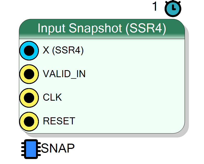
Captures 8192 consecutive SSR4 groups (32768 samples, 32.768 us at 1 GS/s) of the RF input and makes them readable on the bus. Wire X to the same net that feeds the Baseband DDC X pin (Multichannel SigGen OUT) and VALID_IN to its VALID (unconnected VALID_IN = ‘1’, one group every clock).
Pin Description
Properties
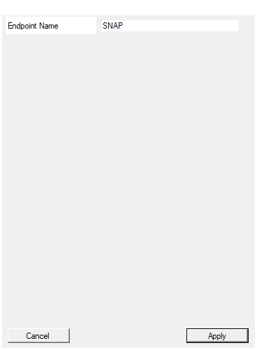
Name of the register endpoint. Registers are REG_
SNAP).
Default: SNAP
Usage
Capture
- write CTRL = 1 (arm): the write pointer and STATUS.done are cleared;
- every clock with VALID_IN = ‘1’ one SSR4 group is stored, linearly from group 0; when the 8192nd group is stored the capture stops (one-shot) and STATUS.done rises;
- read the memory window
DATA. No trigger, no pre-trigger, no decimation, never circular: word 0 is the first sample in time.
Window format (DATA, 16384 words x 32 bit, read-only)
| word | [15:0] | [31:16] |
|---|---|---|
| 2g | lane 0 of group g (oldest sample) | lane 1 |
| 2g+1 | lane 2 | lane 3 (newest) |
| i.e. sample n of the capture is the int16 at word n/2, half n mod 2. |
Registers (endpoint = EndpointName, default SNAP)
| register | access | meaning |
|---|---|---|
CTRL |
W | b0 arm, b1 clr_status: write-1-to-pulse (every write of 1 pulses) |
STATUS |
R | b0 done, b2 busy |
| Bus writes to the window are ignored. A second arm restarts from group 0; | ||
| clr_status clears done only (it does not stop a running capture). |
Resources & Timing
-
Latency: arm to first stored group: 3 clocks (strobe synchroniser) + 2
-
Throughput: 1 SSR4 group (4 samples) per clock
8192 x 64 bit block RAM (16 RAMB36). X and VALID_IN are registered twice before the RAM (timing at 250 MHz with a shared source net). Bus read latency one clock. Verified in GHDL (tb/kria_snapshot).