IDE User Interface
Complete guide to the SCI-Compiler Integrated Development Environment. Learn the starting window for creating and opening projects, explore the main interface layout, understand toolbars and menus, work with the diagram editor, configure hardware settings, and monitor compilation output.
Starting Window
When you launch SCI-Compiler, the Starting Window appears, offering three main options for working with projects.
Purpose
The starting window allows you to:
- Create a new project from scratch
- Open a recent project
- Explore example projects provided with SCI-Compiler
Create Project Tab
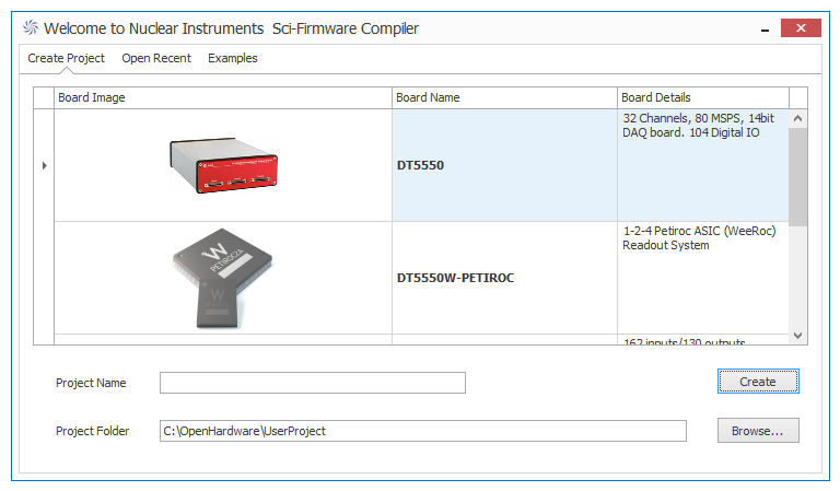
Figure 1: Create Project tab
Creating a New Project
-
Click on a board button to select your target platform:
- V2495 - CAEN VME general-purpose board
- DT5550 - Desktop USB/Ethernet digitizer
- DT5550W - With Weeroc ASIC support (Petiroc/Citiroc)
- DT1260 - Low-cost USB acquisition board
- V2495X - Extended V2495 variant
- Other supported boards
-
Enter a Project Name in the text field
-
Specify the Project Folder path:
- Type the full path manually
- Click Browse… to select via dialog
-
Click Create button
What Gets Created
SCI-Compiler creates a project folder containing:
Files:
- [ProjectName].scf - Project file (SCI-Compiler format)
- [ProjectName].jpg - Diagram preview image (initially empty)
Folders:
- HDL/ - Generated VHDL/Verilog code
- Library/ - RegisterFile.json and SDK files
- Output/ - Compilation outputs and bitstreams
Open Recent Tab
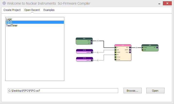
Figure 2: Open Recent tab
Opening Existing Projects
The Open Recent tab provides quick access to your previous work:
Left panel:
- List of recently opened projects (chronological order)
- Click on a project to select it
Right panel:
- Preview image of the selected project’s diagram
- Visual confirmation before opening
Bottom field:
- Full path to the .scf file
- Browse… button to find other project files
Open button:
- Loads the selected project
- Displays diagram in main interface
Examples Tab
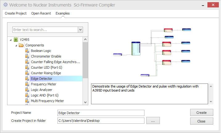
Figure 3: Examples tab
Exploring Example Projects
SCI-Compiler includes pre-built example projects demonstrating various features and techniques.
Left panel - Example browser:
- Organized by board type and application category
- Expand folders to see available examples
- Examples include:
- QDC - Charge-to-Digital Converter
- TDC - Time-to-Digital Converter
- Oscilloscope - Waveform capture
- Spectrum - MCA energy histogram
- Logic Analyzer - Digital signal capture
- Pattern Generator - Test signal generation
- Many more…
Right panel - Preview:
- Block diagram image of selected example
- Description of functionality
- List of features demonstrated
Project configuration:
- Project Name field - Modify if desired
- Create Project in folder - Destination path
- Browse button - Select location
Create button:
- Copies example to your project folder
- Allows customization without affecting original
Using Examples
Examples are fully functional projects you can:
- Open and explore with integrated Help
- Compile to generate bitstream
- Program onto your hardware
- Modify and extend for your needs
- Study to learn design techniques
Main Interface
After creating or opening a project, the main SCI-Compiler IDE appears.
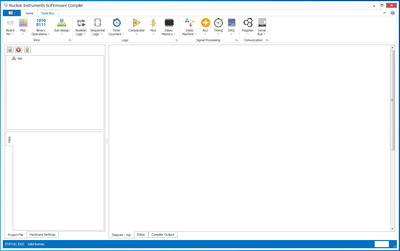
Figure 4: Main interface overview
Interface Organization
The IDE is organized into several key areas:
- File Menu - Project and application management
- Toolbars - Quick access to common functions
- Resources and Settings - Project files and hardware configuration
- Central Area - Diagram, Editor, Compiler Output tabs
- Status Bar - License info, progress indication
Title Bar
At the top of the window:
Nuclear Instruments SciFirmware Compiler - [ProjectName]
Shows the current project name for easy identification.
File Menu
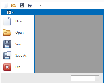
Figure 5: File Menu
Click the blue button in the toolbar region to access the File Menu.
Menu Items
| Item | Function |
|---|---|
| New | Opens Starting Window to create new project |
| Open | Browse and open existing .scf project file |
| Save | Save current project (updates .scf and .jpg) |
| Save As | Save project with new name or location |
| Exit | Close SCI-Compiler application |
Keyboard Shortcuts
- Ctrl+N - New project
- Ctrl+O - Open project
- Ctrl+S - Save project
- Ctrl+Shift+S - Save As
Home Toolbar

Figure 6: Home toolbar
The Home toolbar contains frequently used controls organized into functional groups.
File Group
Same functions as File Menu:
- New - Create new project
- Open - Open existing project
- Save - Save current project
Tools Group
Diagram editing tools:
| Tool | Shortcut | Function |
|---|---|---|
| Copy | Ctrl+C | Copy selected blocks/wires to clipboard |
| Cut | Ctrl+X | Cut selected elements (remove but keep in memory) |
| Paste | Ctrl+V | Paste clipboard contents |
| Undo | Ctrl+Z | Undo last action |
| Redo | Ctrl+Y | Redo previously undone action |
Editor Group
Register and clock management:
| Tool | Function |
|---|---|
| Add | Add single user-defined clock or register |
| Add Multi | Add multiple registers with auto-numbering |
| Delete | Remove selected clock or register |
| Reload | Reset current Editor tab to defaults |
Compiler Group
Compilation and programming tools:
| Tool | Function |
|---|---|
| Compile | Generate VHDL and run FPGA synthesis |
| Program FPGA | Download bitstream to board |
| Settings | Configure compilation paths and options |
| Resource Explorer | Test firmware on connected board |
Compile process:
- Generates VHDL from block diagram
- Creates TCL scripts
- Launches Vivado/Quartus
- Runs synthesis and implementation
- Generates bitstream
- Creates RegisterFile.json
Program FPGA process:
- Connects via JTAG cable
- Downloads bitstream to FPGA
- Verifies programming success
Resource Explorer:
- Connect to board via USB/VME/Optical
- Access registers in real-time
- Test oscilloscopes, spectra, lists
- Monitor hardware without custom software
Tools Box Toolbar

Figure 7: Tools Box toolbar
The Tools Box contains all pre-compiled FPGA blocks, organized by category.
Important: Available blocks depend on the selected board type. Not all blocks are available for all platforms.
Wire Group
Single-wire and bus operations:
Board Pin sub-menu:
- Analog inputs (ADC channels)
- Digital inputs/outputs
- Differential I/O (LVDS)
- Board-specific connectors
Misc sub-menu:
- Constants (integer, boolean, True, False)
- Clocks (board clock, custom frequencies)
- Conversions (binary ↔ decimal, signed ↔ unsigned)
Binary Operations sub-menu:
- Wire Join - Combine multiple signals into bus
- Wire Split - Separate bus into individual signals
- Bit Select - Extract specific bits
- Bit Slice - Extract bit range
Sub-design sub-menu:
- Insert hierarchical sub-design blocks
- Synchronize sub-design files
Logic Group
Digital logic and timing:
Boolean Logic sub-menu:
- AND, OR, XOR, NOT gates
- NAND, NOR, XNOR
- Reduce operations (AND-reduce, OR-reduce, XOR-reduce)
Sequential Logic sub-menu:
- Rising/Falling edge detectors
- D Flip-Flops
- Latches
- Shift registers
Timer Counters sub-menu:
- Rising/Falling edge counters
- Chronometers
- Timers
- Frequency meters
- Scalers
Comparator sub-menu:
- Greater than, less than
- Equal, not equal
- Multi-bit comparators
Mux sub-menu:
- Multiplexers (2:1, 4:1, 8:1, N:1)
- Demultiplexers
Delay Memory sub-menu:
- Delay lines (configurable depth)
- Serializer/Deserializer
- RAM (single/dual port)
- ROM
- FIFOs
- Pattern Generator
Signal Processing Group
Advanced DSP and acquisition:
State Machine sub-menu:
- Finite State Machine designer
- State diagram editor
ALU sub-menu:
- Add, Subtract, Multiply
- Shift, Rotate
- Absolute value, Min, Max
Timing sub-menu:
- TDC (Time-to-Digital Converter)
- SCA (Single Channel Analyzer)
- ToT (Time-over-Threshold)
- Leading/Trailing edge detectors
DAQ sub-menu:
- Oscilloscope (waveform capture)
- Digitizer (continuous streaming)
- Baseline Restorer
- QDC (Charge Integration)
- Trapezoidal Filter
- Trigger Logic
- Logic Analyzer
- Spectrum (MCA histogram)
Communication Group
Interface with registers and protocols:
Register sub-menu:
- Register Read - Read from memory-mapped register
- Register Write - Write to memory-mapped register
Serial Bus sub-menu:
- I2C Master/Slave
- SPI Master/Slave
- UART (RS-232)
Board-Specific (depending on platform):
- Petiroc/Citiroc Slow Control
- HV Controller
- Custom interfaces
Resources and Settings
The left panel provides project management and hardware configuration.
Project File Tab
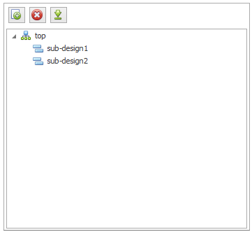
Figure 8: Project File tab
Top section - File tree:
Shows project structure in tree view:
Main design - Top-level project file
Sub-design - Hierarchical sub-modules
Click on a file to:
- Display its diagram in the Diagram area
- Show Tools Box toolbar
- Enable editing
File management buttons:
| Button | Function |
|---|---|
|
Create new sub-design file |
|
Delete selected sub-design |
|
Synchronize sub-design for use as block |

Bottom section - Help panel:
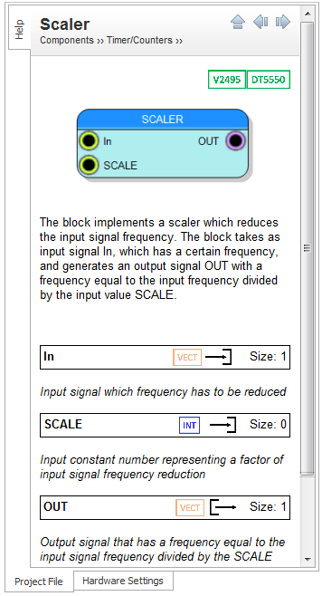
Figure 9: Integrated Help panel
Click any block in the diagram to display:
- Block name and category
- Board compatibility badge:
or

- Block image/symbol
- Functional description
- Input/output signal table
Signal information includes:
- Signal name
- Data type:
or

- Direction:
or

- Bit width
- Brief description
Navigate help topics using arrow buttons at the top.
Diagram Tab
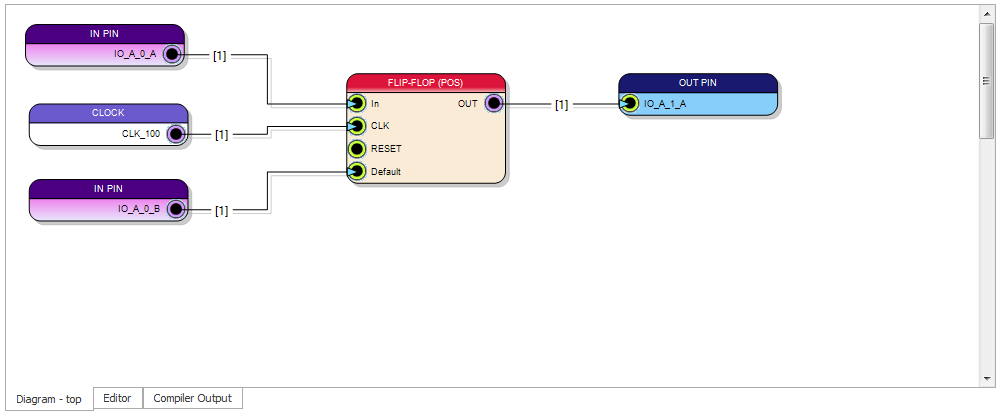
Figure 10: Diagram editor
The Diagram is the main graphical design area where you create FPGA firmware.
Working in the Diagram
Adding blocks:
- Select block from Tools Box toolbar
- Click in Diagram to place
- Block appears with default properties
Connecting blocks:
- Click on output circle of source block
- Drag to input circle of destination block
- Wire is created if types match
Wire properties:
- Arrow indicates signal direction
- [N] shows bus width (number of bits)
- Color indicates signal type:
- Black - Standard logic
- Blue - Integer
- Red - Error (type mismatch)
Connection Rules
Valid connections:
- Output type must match input type (integer or vector)
- Output width must match input width
- One output can connect to multiple inputs (fan-out)
- One input can connect to only one output
Invalid connections:
- Type mismatch (integer → vector or vice versa)
- Width mismatch (8-bit → 16-bit without conversion)
- Multiple drivers on single input
Compilation requirements:
- Main inputs/outputs must be connected
- Unconnected optional inputs receive defaults:
- RESET → Global reset signal
- CLK → Board clock
- GATE → Constant ‘1’ (enabled)
Keyboard Shortcuts
Efficient diagram editing with shortcuts (see Shortcuts section):
- Alt+R - Replicate connection
- Alt+F - Fan-out from source
- Alt+E - Fan-out to destinations
- Alt+S - Serial connection
- Ctrl+Drag - Pan diagram
- Mouse Wheel - Zoom in/out
Project Settings Tab
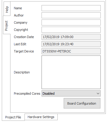
Figure 11: Project Settings
Project Information
Define project metadata:
- Project Name - Display name
- Author - Creator name
- Description - Project summary
- Version - Project version number
Precompiled Cores
Enable Precompiled Cores option:
When enabled:
- ✓ Faster compilation (5-10x speedup)
- ✓ Reduced compilation time
- ✓ Stable, tested IP cores
- ✗ Limited source code visibility (closed IP)
- ✗ Requires Vivado 2017.4 or compatible
When disabled:
- ✓ Full open-source VHDL available
- ✓ Complete code transparency
- ✓ Easier debugging and modification
- ✗ Longer compilation time
- ✗ Requires more FPGA resources
Recommendation:
- Production use: Enable for faster iterations
- Learning/Research: Disable for full code access
Board Configuration Tab
Configure hardware-specific I/O settings.
DT5550 I/O Configuration
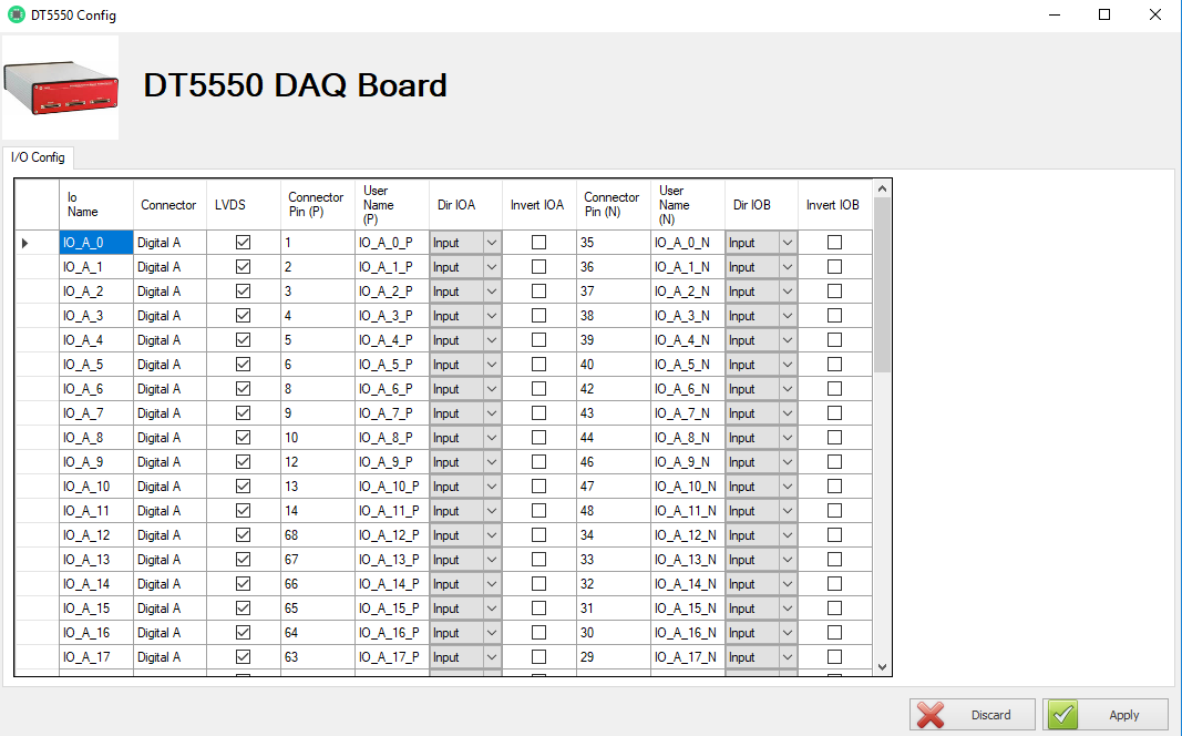
Figure 12: DT5550 bank connector configuration
Digital I/O (48 channels):
- Select Input or Output direction
- Enable LVDS for differential signaling
- Invert signal polarity if needed
Configured pins appear in Board Pin menu for use in diagram.
V2495 I/O Configuration
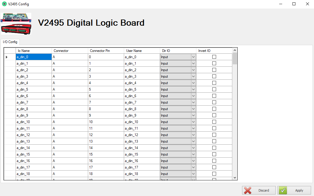
Figure 13: V2495 connector configuration
Connector types:
- A, B connectors - Input only (fixed)
- C connectors - Output only (fixed)
- D, E, F connectors - Configurable (input or output)
Options:
- Invert - Invert signal polarity
DT5550W Petiroc Configuration
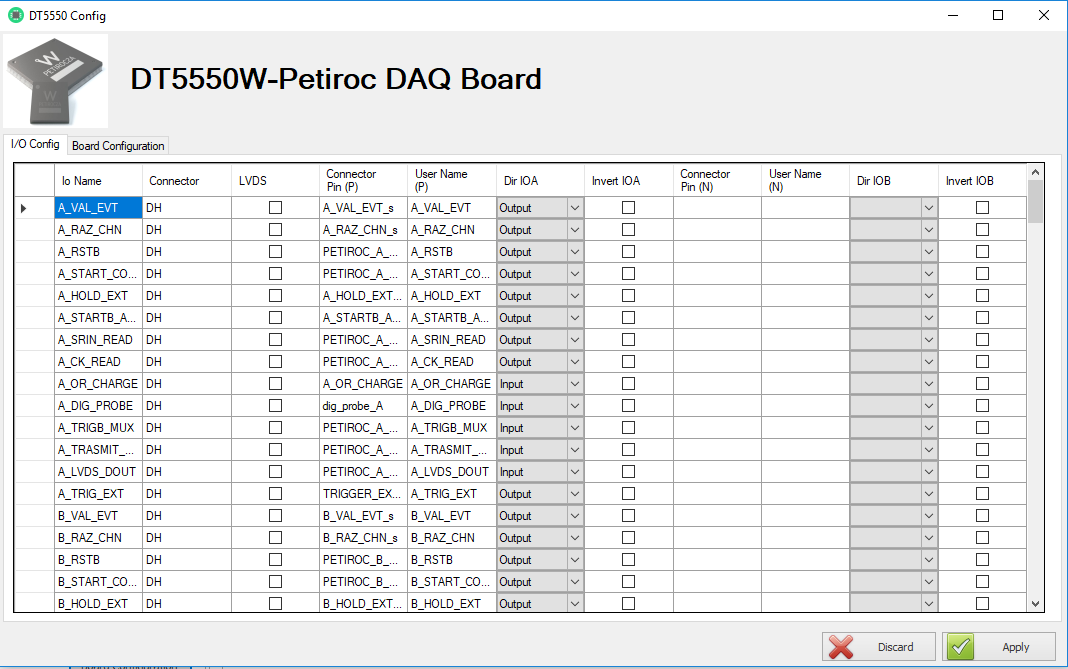
Figure 14: DT5550W Petiroc pin configuration
Pin configuration:
- All pin directions are fixed (hardware-defined)
- No single-ended/differential selection
- Pins are pre-configured for Petiroc ASIC interface
ASIC Clock Control:
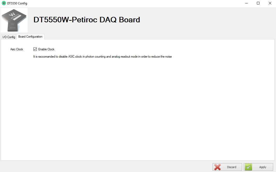
Figure 15: Enable/Disable ASIC clock
Enable or disable clock to Petiroc/Citiroc ASIC:
- Disable clock for ultra-low noise in photon counting
- Disable clock during analog readout
- Enable clock for digital readout and fast triggers
Compiler Output Tab

Figure 16: Status bar showing compilation progress
Viewing Compiler Output
The Compiler Output section displays messages from:
- SCI-Compiler operations
- Vivado/Quartus synthesis tool
- FPGA programming process
Automatically displayed when:
- Compile button pressed
- Program FPGA button pressed
Manually accessible:
- Click Compiler Output tab
Message Color Coding
| Color | Meaning |
|---|---|
| Blue | SCI-Compiler operations (project creation, file generation) |
| Black | Vivado/Quartus output (synthesis, implementation) |
| Orange | Warning messages (non-critical issues) |
| Red | Error messages (compilation failures) |
Typical Messages
Project operations (Blue):
Creating project folder: C:\Projects\MyDesign
Generating VHDL files...
Creating RegisterFile.json
Synthesis output (Black):
Synthesis started...
Elaborating entity <design_1_wrapper>
Synthesizing module <design_1>
Finished synthesis
Warnings (Orange):
WARNING: Signal 'unused_signal' has no load
WARNING: Timing constraint not met (slack -0.123 ns)
Errors (Red):
ERROR: Signal 'data_in' has multiple drivers
ERROR: Port 'clk' is not connected
Status Bar
The bottom status bar shows real-time information about SCI-Compiler state.
Status Indicators
Status label (left):
- IDLE - No process running, ready for commands
- COMPILING - Firmware compilation in progress
- PROGRAMMING - FPGA programming in progress
- SIMULATING - Simulation running
Progress bar (right):
- Shows completion percentage of current operation
- Animated during compilation/programming
- Includes time estimate
License label (center):
- Shows license number
- Displays maximum supported software version
- Indicates license validity
License format:
License: 12345-67890 | Version: ≤ 2.5.0
License errors:
- “License not found” - USB dongle not connected
- “License expired” - Version too new for license
- “Invalid license” - Corrupted or tampered dongle
For license issues, see SCI-Compiler License section.
Best Practices
Project Organization
- Use descriptive names - Clear project and file names
- Create sub-designs - Modularize complex designs
- Save frequently - Protect work with Ctrl+S
- Use version control - Track .scf files with Git
Diagram Design
- Keep diagrams clean - Avoid wire tangles
- Use labels - Name important signals
- Group related blocks - Logical organization
- Add comments - Document design intent
Compilation
- Check messages - Review warnings and errors
- Fix warnings - Don’t ignore orange messages
- Verify timing - Check timing reports
- Test incrementally - Compile often during development
Resource Explorer Usage
- Test before SDK - Verify with Resource Explorer first
- Monitor registers - Real-time debugging
- Save configurations - Export register settings
- Document results - Screenshot successful tests
Common Workflows
Creating New Firmware
- File → New → Select board
- Add blocks from Tools Box
- Connect signals
- Configure registers (Memory Mapping tab)
- Compile
- Program FPGA
- Test with Resource Explorer
Modifying Existing Design
- File → Open Recent → Select project
- Review diagram and Help
- Make changes
- Save (Ctrl+S)
- Compile
- Compare RegisterFile.json changes
- Program FPGA
- Re-test functionality
Learning from Examples
- Starting Window → Examples tab
- Browse categories
- Select interesting example
- Create copy to your folder
- Study diagram structure
- Read block Help
- Compile and test
- Modify and experiment
Hierarchical Design
- Create sub-design:

- Design sub-module in new tab
- Synchronize:

- Add to main design via Sub-design menu
- Connect as regular block
Summary
The SCI-Compiler IDE provides a complete graphical environment for FPGA firmware development:
| Component | Function |
|---|---|
| Starting Window | Create, open, or explore projects |
| File Menu | Project management |
| Home Toolbar | Quick access to common operations |
| Tools Box | Library of FPGA blocks |
| Project File | File hierarchy and integrated Help |
| Diagram | Graphical firmware design |
| Board Configuration | Hardware I/O settings |
| Compiler Output | Synthesis and programming messages |
| Status Bar | License, progress, and state |
Key advantages:
- Visual design - No HDL coding required
- Integrated help - Context-sensitive documentation
- Pre-built blocks - Extensive IP library
- Real-time feedback - Instant error checking
- Complete workflow - Design through testing in one tool
Master the IDE to unlock the full power of SCI-Compiler!