H-LINK
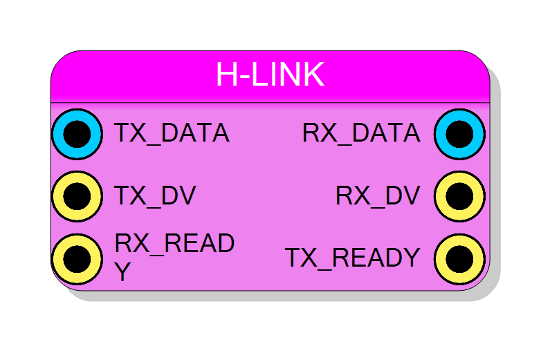
Board pin block that exposes one of the two R5560 / R5560SE board-to-board high-speed links to the diagram as a pair of 64-bit AXI-Stream ports - one receive, one transmit. The link itself is an Aurora 64B/66B core on a GTX transceiver inside the board’s block design; the block is the wiring to the asynchronous FIFOs that cross into your clock domain.
Introduction
Principle of Operation
H-LINK is the R5560 family’s board-to-board serial link. Two of them exist on each board - conventionally the RIGHT and the LEFT neighbour
- so a row of boards can be daisy-chained and exchange data without going through the host.
The link itself is not built by this block. In the board’s Zynq block design
each H-LINK is a Xilinx Aurora 64B/66B core (aurora_64b66b v11.2) on a
GTX transceiver lane, with an AXI-Stream data FIFO on each side to cross
between the Aurora user clock and the design clock:
┌──────────── board block design ────────────┐
your diagram │ │
TX_DATA ─64─┬───────► │ axis_data_fifo ──► Aurora 64B/66B ──► GT TX │ ──► cable
TX_DV ─────┤ (async) │ │
TX_READY ◄──┘ │ │
│ │
RX_DATA ◄─64─┬────── │ axis_data_fifo ◄── Aurora 64B/66B ◄── GT RX │ ◄── cable
RX_DV ◄────┤ (async)│ │
RX_READY ────┘ └────────────────────────────────────────────┘
What you see in the diagram is therefore a plain AXI-Stream pair: 64-bit data, a valid, and a ready, in each direction. The block adds no framing, no packetisation, no error reporting and no back-pressure logic of its own.
Pin Description
Word to transmit. Assigned to HLINK{id}_FIFO_IN_tdata.
Must be held stable while TX_DV is high and TX_READY is low.
The assignment is emitted unconditionally, so this pad must be wired.
Transmit valid. Assigned to HLINK{id}_FIFO_IN_tvalid. Assert for
each word you want to send and keep it asserted until the cycle where
TX_READY is also high.
If left unconnected the plug-in substitutes the literal "0", so the
transmit direction is permanently idle.
Receive ready - your back-pressure towards the link. Drives
HLINK{id}_FIFO_OUT_tready. Drop it low to hold words in the board’s
receive FIFO.
If left unconnected the plug-in substitutes the literal "1", i.e. the
design claims to accept a word on every cycle. That is the right default
only if your consumer really is always ready; otherwise words are handed
over and dropped on the floor.
Received word. Driven from HLINK{id}_FIFO_OUT_tdata. Valid on the
cycles where RX_DV is high; meaningless otherwise.
Already in your clock domain - the board’s receive FIFO is the asynchronous crossing.
The assignment is emitted unconditionally, so this pad must be wired.
Receive valid (HLINK{id}_FIFO_OUT_tvalid). High when RX_DATA
carries a word the link wants to hand over. A transfer happens on the
clock edge where RX_DV and RX_READY are both high.
Safe to leave unconnected - the plug-in guards this assignment and simply omits it. Doing so means you have no way of knowing when data arrives, so it is only sensible if you do not use the receive direction at all.
Transmit ready (HLINK{id}_FIFO_IN_tready). High when the board’s
transmit FIFO can accept a word this cycle. Your TX_DATA / TX_DV must
stay stable until a cycle where this is high.
Safe to leave unconnected - the assignment is guarded and omitted. If you ignore it you are streaming blind: any word offered while the FIFO is full is lost.
Properties
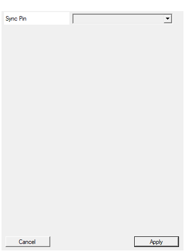
Set sync pin to use for this block
Which of the two links this block drives, despite the name and the
Sync Pin label - both are copy-paste leftovers from the sibling Sync
blocks in this plug-in.
| Value | Link index | Board signals | Aurora core / transceiver |
|---|---|---|---|
RIGHT |
0 | HLINK0_FIFO_* |
HLINK_0 on GT_RX_2 / GT_TX_2 |
LEFT |
1 | HLINK1_FIFO_* |
HLINK_1 on GT_RX_3 / GT_TX_3 |
The selection is a simple = "RIGHT" test in CompileHDL; every other
value, including the block’s own out-of-list default SYNC_0, resolves
to LEFT. Set it explicitly.
RedesignIfChanged is set (the pin list itself does not change) and it
can be changed after the block is created.
Default: SYNC_0 (not a legal list value - behaves as LEFT)
Default: SYNC_0
Options: RIGHT LEFT
⚙️ Detailed Operation
What the block compiles to
The Sync Pin property (see the trap below - it selects the link, not a
sync) picks the link index id: RIGHT gives id = 0, anything else gives
id = 1. The plug-in then emits six assignments against HLINK{id}_*:
<RX_DATA> <= HLINK0_FIFO_OUT_tdata;
<RX_DV> <= HLINK0_FIFO_OUT_tvalid; -- only if the pad is connected
HLINK0_FIFO_OUT_tready <= <RX_READY>;
HLINK0_FIFO_IN_tdata <= <TX_DATA>;
HLINK0_FIFO_IN_tvalid <= <TX_DV>;
<TX_READY> <= HLINK0_FIFO_IN_tready; -- only if the pad is connected
plus one informational line in the compiler output:
Generating HDL code for <designator>
Two of the input pads carry a default value used when you leave them unconnected:
TX_DVdefaults to"0"- nothing is transmitted;RX_READYdefaults to"1"- the design always accepts.
Two of the output pads (RX_DV, TX_READY) are guarded and simply produce
no assignment when unwired. RX_DATA and TX_DATA are not guarded.
The handshake
This is standard AXI-Stream, and it is worth being explicit because the block does not enforce it for you:
- Transmit. A word is taken by the link on the clock edge where
TX_DV = '1'andTX_READY = '1'. You must holdTX_DATAandTX_DVstable until that happens - droppingTX_DVbecauseTX_READYis low loses nothing, but changingTX_DATAwhileTX_DVis high andTX_READYis low corrupts the word that is waiting. - Receive. A word is delivered on the clock edge where
RX_DV = '1'andRX_READY = '1'. If you tieRX_READYhigh (or leave it unconnected, which does the same) you must consumeRX_DATAon every cycleRX_DVis high, because the FIFO will keep advancing.
The board side
In the R5560 top-level template the twelve HLINK0_* / HLINK1_* signals
are declared as 64-bit / 1-bit vectors with "0" defaults and port-mapped
into the Zynq block design wrapper. Inside the block design:
HLINK_0is anaurora_64b66bcore on GT_RX_2 / GT_TX_2;HLINK_1is anaurora_64b66bcore on GT_RX_3 / GT_TX_3, sharingHLINK_0’s QPLL, reference clock, sync clock and MMCM lock;- each direction of each link goes through an
axis_data_fifoconfiguredTDATA_NUM_BYTES = 8(64 bit) andIS_ACLK_ASYNC = 1; - the user side of all four FIFOs is clocked by
CLOCK_PL- the design clock - while the Aurora side runs on the Aurorauser_clk_out.
So the clock-domain crossing is done for you, and RX_DV / TX_READY are
already in your clock domain. No extra synchroniser is needed on these pins.
What the block does not give you
- No link status. Aurora’s channel-up, lane-up, hard-error and soft-error signals are not brought out to any pin of this block. From inside the diagram you cannot tell whether the link is trained.
- No framing. Aurora here is used in streaming mode as far as this
interface is concerned; there is no
tlast, no packet length and no start-of-frame. Any message boundary has to be encoded in the 64-bit words themselves. - No loopback or self-test.
Typical use
- Daisy-chaining trigger or hit data between adjacent boards in a crate.
- Forwarding a partially processed event stream to a neighbour that does the next stage.
- Building a token ring across a row of boards, one word per token.
Board availability
SupportedBoard is GUID_BASED, and SupportedBoardGuids names two boards:
| Board GUID | Board plug-in |
|---|---|
F417C046-3AA0-4E63-964A-2008A6D35172 |
R5560 (boards/ni/board_R5560/bR5560.vb) |
C75E5DBB-6827-46A2-88BB-DBF38A36AAD7 |
R5560SE (boards/ni/board_R5560SE/bR5560SE.vb) |
No other board plug-in in the repository declares HLINK0_* / HLINK1_*
signals, so the block is meaningless anywhere else - and the toolbox will not
offer it.
This block is flagged as available inside sub-designs and inside state machines.
Resources & Timing
-
Latency: Not determined from these sources - the round trip is dominated by the Aurora 64B/66B core and by two asynchronous AXI-Stream FIFOs, neither of which states a figure here.
-
Throughput: One 64-bit word per design clock at the interface, subject to the AXI-Stream handshake; the sustained rate is limited by the GTX line rate, which is not stated in these sources.
- The block itself costs nothing: it compiles to six concurrent assignments. All the logic is already in the board’s block design.
- Both directions are already clock-domain-crossed into
CLOCK_PL(axis_data_fifowithIS_ACLK_ASYNC = 1); do not add your own synchroniser onRX_DV/TX_READY. - The two Aurora cores share a QPLL, a reference clock and an MMCM lock, so they come up and go down together.