
FFT Windowed TM Prog
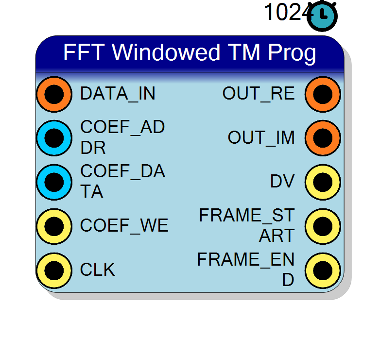
Runtime-programmable variant of FFT Windowed TM: the same gapless polyphase TM FFT with an in-line window multiplier, but the window coefficients live in RAM and are written at run time through a small COEF_ADDR / COEF_DATA / COEF_WE bus instead of being baked in by the designer. Rectangular (all ones) until loaded. No custom GUI - the four hardware properties are plain combo boxes.
Introduction
Principle of Operation
This block is FFT Windowed TM with a writable window. The datapath is
generated by the same code (Component_FFTWindowedTM.SharedCompileHDL, called
with programmable = True), so everything the FFT Windowed TM page says about
the transform holds here too:
- the TM input carries $R$ samples per clock ($R$ = TMFactor, 2 or 4);
- each lane is multiplied by its own polyphase slice of the window, $\mathrm{WROM}_r[m] = w[mR + r]$;
- the windowed lanes feed the gapless polyphase FFT engine (one Xilinx
xfftcore of $M = N/R$ points plus the multiplier-free recombination), and $R$ spectrum bins come out per clock, back to back.
The only difference is where $w[n]$ comes from:
| FFT Windowed TM | FFT Windowed TM Prog | |
|---|---|---|
| Window storage | VHDL constant ROM |
VHDL signal RAM |
| Set by | the FFT Windowed designer (double-click) | the COEF_* bus, at run time |
| Value before load | the designed window | rectangular (0xFFFF in every cell) |
| Extra pins | – | COEF_ADDR, COEF_DATA, COEF_WE |
| Properties | FFTLength, TMFactor, InputBits, ScalingMode, Window, WFProject | FFTLength, TMFactor, InputBits, ScalingMode |
Use it when the window has to change without re-running synthesis: adaptive spectral analysis, a window selected by the operator, or a measurement that sweeps several windows over the same acquisition.
To design a window, place a fixed FFT Windowed block, use its designer to
preview the shape, and export the coefficient list; then drive those values into
this block’s COEF_* bus from your own loader (a state machine, a register
file, a soft core).
Pin Description
InputBits each,
packed lane 0 in the least significant field. This is the only data input;
samples are consumed every clock (no clock enable, no back-pressure).
0 … N-1,
ceil(log2 N) bits. The wrapper derives the polyphase lane
($n \bmod R$) and the RAM index ($\lfloor n/R \rfloor$) internally.
65535 = 1.0, 0 = 0.0.
Negative coefficients are not representable.
COEF_DATA at COEF_ADDR.
Takes effect on the next sample, with no frame boundary interlock.
outBits per bin
(see the Output width table). Bins come out in natural order, frames back
to back.
OUT_RE.
Properties
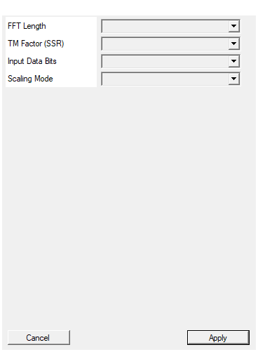
Transform length N (power of 2)
Transform length $N$, a power of two. Available values: 64, 128, 256, 512, 1024, 2048, 4096, 8192, 16384. The instantiatedxfft core is $N/\text{TMFactor}$ points, and the window
RAM holds $N$ coefficients spread over TMFactor polyphase banks.
Default: 1024
Default: 1024
Options: 64 128 256 512 1024 2048 4096 8192 16384
Time Multiplexing factor (samples per clock). 2 or 4 (multiplier-free recombination).
Time-multiplexing factor $R$ = samples per clock onDATA_IN and bins per
clock on OUT_RE / OUT_IM.
Available values: 2, 4 — nothing else compiles (the recombination
stage is multiplier-free only for these two).
Default: 4
Default: 4
Options: 2 4
Bit width of each input sample (8-24 bits)
Bit width of one input sample, 8 … 24. It is also theinput_width of the
generated xfft IP and the width the windowed sample is rounded back to.
Default: 16
Default: 16
Options: 8 9 10 11 12 13 14 15 16 17 18 19 20 21 22 23 24
No Scaling: full bit growth (InputBits + log2(N) + 1). Grow to Max: saturated to 27 bits. Scale: output divided by N, InputBits wide (saturated).
How the FFT core handles bit growth.
| Value | Output width | Meaning |
|---|---|---|
| No Scaling | $\min(\text{InputBits}+\lceil\log_2 N\rceil+1, 32)$ | full bit growth, no loss |
| Grow to Max | $\min(\text{InputBits}+\lceil\log_2 N\rceil+1, 27)$ | grown then saturated to 27 bit |
| Scale | InputBits |
divided by $N$, saturated back to the input width |
Default: No Scaling
Default: No Scaling
Options: No Scaling Grow to Max Scale
⚙️ Loading the window
The load port is a plain synchronous write port on the polyphase RAMs. One coefficient per clock:
COEF_ADDR <= n -- n = SAMPLE index, 0 .. N-1
COEF_DATA <= round(w[n] * 65535) -- unsigned Q16
COEF_WE <= '1' -- one clock
COEF_ADDR is ceil(log2 N) bits wide. The address is split inside the
wrapper exactly as the polyphase decomposition requires — you do not have to
do that split yourself:
$$ \text{lane } r = n \bmod R \qquad \text{ROM index } m = \left\lfloor n / R \right\rfloor $$
(the low $\log_2 R$ bits of COEF_ADDR select the lane, the remaining bits are
the index inside that lane’s RAM). Writing n = 0 … N-1 in natural order
therefore loads the window in natural order.
Until the first write the RAMs are initialised to (others => '1'), i.e.
0xFFFF in every cell: the block behaves as an unwindowed (rectangular)
gapless FFT.
The window multiplier
Per lane $r$, in two registered stages:
vhdl
x0(r) <= signed(data_in((r+1)*inBits-1 downto r*inBits));
w0(r) <= WROM_r(to_integer(m_cnt));
p1(r) <= x0(r) * signed('0' & w0(r));
...
core_in((r+1)*inBits-1 downto r*inBits)
<= std_logic_vector(resize(shift_right(p1(r) + 32768, 16), inBits));
so the windowed sample is
$$ x_w[n] ;=; \left\lfloor \frac{x[n],w[n] + 2^{15}}{2^{16}} \right\rfloor $$
— a round-to-nearest back to InputBits, not a truncation. Because
$w[n] \le 65535 < 2^{16}$ the magnitude never grows, so the resize cannot
overflow and no saturation logic is needed. The cost is one DSP slice per lane.
Window phase
m_cnt is a free-running counter reloaded only by the global reset; its
initial value compensates the 2-stage window pipeline against the 3 startup
tready drops of the xfft core in pipelined-streaming mode
(WINIT = ((2 - 3) mod M + M) mod M, i.e. $M-1$). The consequence for the
user is simple:
- the window is aligned to frames by reset, not by any input signal;
- there is no
START/ frame-trigger pin — frames are back to back from reset on, andFRAME_START/FRAME_ENDtell you where they fall.
The source comments state that this offset was verified in xsim and must be
re-verified if the xfft IP version changes.
Output width
OUT_RE / OUT_IM are TM buses of outBits per lane, where
| ScalingMode | outBits |
|---|---|
| No Scaling | $\min(\text{InputBits} + \lceil\log_2 N\rceil + 1,\ 32)$ |
| Grow to Max | $\min(\text{InputBits} + \lceil\log_2 N\rceil + 1,\ 27)$ |
| Scale | InputBits (output divided by $N$, saturated) |
Generated hardware
CompileHDL writes into the project’s pcores/ folder:
xfft_wtmp_<designator>.tcl— one Xilinx xfft IP oftransform_length$M = N/R$,pipelined_streaming_io,input_width = InputBits,phase_factor_width 16,scaling_options unscaled,rounding_modes convergent_rounding,output_ordering natural_order,aresetn true;ssr_fft_wtmp_<designator>.vhd— the polyphase gapless wrapper (shared with FFT TM Realtime);fft_wtmp_<designator>.vhd— the top level: window RAMs, the load port, the multiplier stage and the core instance.
The block is declared _ANY_XLX, i.e. Xilinx targets only.
Constraints and failure modes
-
TMFactormust be 2 or 4. Anything else aborts the compile with<designator>: FFT Windowed TM supports TM factor 2 or 4 only. Selected: <R> -
FFTLength,TMFactor,InputBitsandScalingModeall haveRedesignIfChanged = True: changing any of them re-draws the symbol (pin widths change) and re-generates the IP. -
The block is not available inside a state machine (
AvailableInStateMachine = False); it is available in sub-designs. -
There is no
RESETpin on the symbol:resetis wired automatically to the project global reset, andclkdefaults to the project acquisition clock.
Resources & Timing
- Latency: The symbol declares a latency of N clocks (bxs.Latency = N). The exact cycle-accurate figure is not stated anywhere in the sources; treat N as the figure the compiler uses for automatic delay matching.
- Xilinx only (
SupportedBoard = _ANY_XLX); onexfftcore of N/R points. - One DSP slice per TM lane for the window multiply.
- Window RAM: TMFactor banks of N/TMFactor x 16 bit (N coefficients in total).
- Not available inside a state machine; available in sub-designs.