
QDC/PSD HLS TM
Time-multiplexed charge integration (QDC) with optional Pulse Shape Discrimination (PSD) implemented in HLS. Processes multiple samples per clock cycle for high-speed ADC systems with configurable trigger accuracy.
Introduction
The QDC/PSD HLS TM block implements digital charge integration (QDC) with optional Pulse Shape Discrimination (PSD) for particle identification in time-multiplexed (TM) systems.
This block is designed for high-speed ADC systems where multiple samples are processed per clock cycle. It supports TM factors of 2, 4, 8, 16, or 32 samples per clock.
PSD is used to distinguish different particle types (e.g., neutrons vs. gammas) based on their scintillation pulse shape. Different particles produce different light decay time constants in scintillators, allowing discrimination by comparing charge integrated over different time windows.
The block provides:
- Qlong: Total charge integrated over the long gate
- Qshort: Charge integrated over the short gate (fast component)
- PSD: Ratio of Qshort/Qlong or Qlong/Qshort (selectable)
The core uses Xilinx HLS for efficient FPGA implementation.
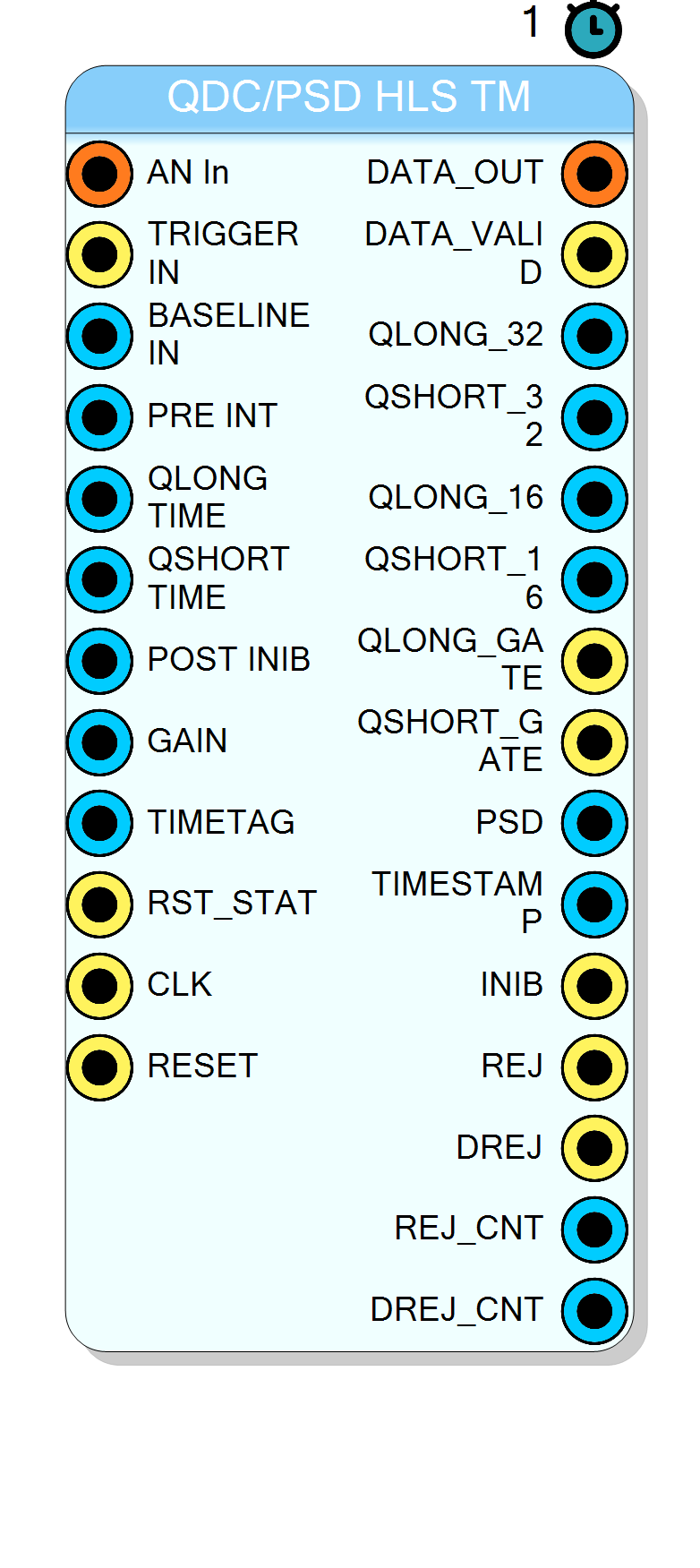
Pin Description
Trigger input pulse.
- In SIMPLE mode: 1-bit signal, starts integration for all TM phases
- In TM mode: TM-bit vector, individual trigger per phase HIGH for one clock/sample when pulse is detected.
Properties
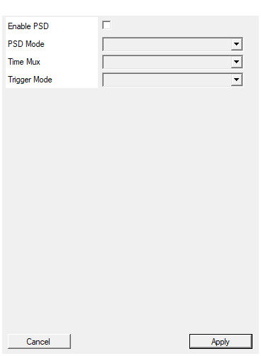
Default: False
Select PSD calculation mode
Default: Qlong/Qshort
Options: Qlong/Qshort Qshort/Qlong
Set number of samples for each clock cycle
Number of samples processed per clock cycle. Determines the time-multiplexing factor. Available values: 2, 4, 8, 16, 32, default 4.Default: 4
Options: 2 4 8 16 32
Select if trigger is SIMPLE or TM
Trigger input mode selection.
- SIMPLE: Single-bit trigger starts integration for all TM phases simultaneously. Timing accuracy is one system clock cycle.
- TM: TM-bit trigger vector allows individual phase triggering. Timing accuracy is one sample period (1/TM of clock cycle). When set to TM, additional outputs QLONG_GATE_TM and QSHORT_GATE_TM become available. Available values: SIMPLE, TM, default SIMPLE.
Default: SIMPLE
Options: SIMPLE TM
PSD calculation mode.
- Qlong/Qshort: PSD = (Qlong / Qshort) * 2^32
- Qshort/Qlong: PSD = (Qshort / Qlong) * 2^32 Available values: Qlong/Qshort, Qshort/Qlong, default Qlong/Qshort.
Usage
PSD Principle
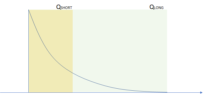
The figure illustrates the pulse shape discrimination principle:
- Qlong integrates the full pulse (PRE_INT to QLONG_TIME after trigger)
- Qshort integrates only the fast component (PRE_INT to QSHORT_TIME after trigger)
- The ratio between these charges discriminates particle types
PSD Simulation Example
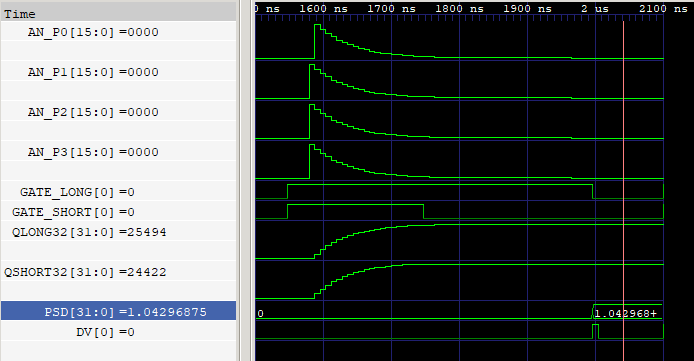
The simulation shows typical PSD waveforms with Qlong and Qshort integration gates.
Time-Multiplexed Processing
In TM mode, the block processes multiple samples per system clock cycle:
| TM Factor | Samples/Clock | Effective Sample Rate |
|---|---|---|
| 2 | 2 | 2x clock frequency |
| 4 | 4 | 4x clock frequency |
| 8 | 8 | 8x clock frequency |
| 16 | 16 | 16x clock frequency |
| 32 | 32 | 32x clock frequency |
Important: The interpretation of integration time parameters (PRE_INT, QLONG_TIME, QSHORT_TIME, POST_INIB) depends on the Trigger Mode:
- SIMPLE mode: Parameters are in clock cycles (all TM phases integrate together)
- TM mode: Parameters are in sample counts (each phase integrates independently)
Trigger Mode Selection
The Trigger Mode property controls how the trigger input is interpreted:
| Mode | Trigger Input | Timing Accuracy | Description |
|---|---|---|---|
| SIMPLE | 1-bit signal | TM group | Single trigger signal starts integration for all TM phases simultaneously. Timing resolution equals one system clock cycle. |
| TM | TM-bit vector | Single sample | Individual trigger for each TM phase. Timing resolution equals one sample period (1/TM of clock cycle). |
SIMPLE Mode:
- Trigger input is a single bit
- When triggered, integration starts at the same point for all TM phases
- Simpler to use with external trigger sources
- Timing accuracy: 1 system clock cycle
TM Mode:
- Trigger input is a vector with one bit per TM phase
- Each phase can trigger independently
- Provides maximum timing accuracy
- Additional outputs: QLONG_GATE_TM, QSHORT_GATE_TM (per-phase gate signals)
- Timing accuracy: 1 sample period (1/TM of clock cycle)
PSD Calculation Modes
The PSD value can be calculated using two formulas, selectable via the PSD Mode property:
Mode 1: Qlong/Qshort (default)
$$ \text{PSD} = \frac{Q_{\text{long}}}{Q_{\text{short}}} \times 2^{32} $$
Mode 2: Qshort/Qlong
$$ \text{PSD} = \frac{Q_{\text{short}}}{Q_{\text{long}}} \times 2^{32} $$
The choice depends on the application:
- Qlong/Qshort: Larger values for particles with slower decay (e.g., neutrons in organic scintillators)
- Qshort/Qlong: Complementary ratio, may be preferred for some analysis methods
Integration Timing
The charge integration windows are defined as:
Trigger
|
v
|--PRE_INT--|------------------QLONG_TIME-----------------|--POST_INIB--|
|--------QSHORT_TIME--------|
^ ^ ^
| | |
Integration Qshort ends Ready for
starts next event
- PRE_INT: Samples to include before the trigger (captures rising edge)
- QLONG_TIME: Duration of long integration gate after trigger
- QSHORT_TIME: Duration of short integration gate after trigger
- POST_INIB: Additional dead time after Qlong for pile-up rejection
All timing values are in sample counts (not clock cycles).
Pile-Up Rejection
The block implements non-paralyzable pile-up rejection:
| Event Timing | Behavior |
|---|---|
| Trigger during QLONG window | Both events rejected (REJ flag) |
| Trigger during POST_INIB | Only second event rejected (DREJ flag) |
| Trigger after POST_INIB | Both events accepted normally |
Rejection counters (REJ_CNT, DREJ_CNT) track discarded events for rate analysis.
Output Formats
The block provides charge values in two formats:
| Output | Bits | Gain Applied | Use Case |
|---|---|---|---|
| QLONG_32 / QSHORT_32 | 32 | No | Full resolution for analysis |
| QLONG_16 / QSHORT_16 | 16 | Yes | Reduced data for histogramming |
The GAIN parameter scales the 32-bit values to fit in 16 bits:
$$ Q_{16} = \frac{Q_{32} \times \text{GAIN}}{65536} $$
Baseline Subtraction
The BASELINE IN input allows real-time baseline subtraction:
$$ Q = \sum_{i=0}^{N} (x[i] - \text{baseline}) $$
Connect a baseline restorer block output to remove DC offset and improve energy resolution.
Timing and Latency
- Processing latency: 1 clock cycle
- Throughput: TM samples per clock cycle
Typical Applications
- High-speed neutron/gamma discrimination with fast scintillators
- Multi-GSPS ADC systems
- Phoswich detector readout at high rates
- Time-of-flight measurements requiring precise timing
- PET systems with high count rates