
Citiroc Analog
Analog readout sequencer for one CITIROC 1A ASIC on the DT5550W-Citiroc1A board. On a trigger it closes the hold on the HG/LG peak detectors, then shifts the 32 channel charges out of the ASIC into the board ADC and publishes them three ways at once: a serial channel-by-channel stream, 32 parallel HG/LG/HIT pin triplets, and a single packed 1024-bit frame word for the Citiroc Frame Transfer block.

Introduction
Principle of Operation
The CITIROC 1A holds the peak charge of its 32 channels in two analog memories,
a high-gain (HG) and a low-gain (LG) one. Those memories are not addressable:
the chip exposes them through an internal shift register that is advanced one
position per clock on SR_IN / SCLK, and the currently selected channel is
presented on a single analog output that the board digitises with an external ADC.
This block owns that whole sequence for one ASIC (A, B, C or D):
- detect the rising edge of
TRIG; - wait
HOLD_TIMEclock cycles so the shaper reaches its peak; - assert
HOLD_HG/HOLD_LG, freezing the analog memories; - reset and then step the ASIC charge shift register, one slot at a time;
- sample the (filtered) ADC word at each slot;
- release the hold, run the channel-reset (
RAZ_CHN) sequence and return to idle.
The ADC is never read raw. A 32-tap running boxcar is applied continuously to both ADC inputs, and the readout stores the filtered value:
$$ \widehat{E}[n] ;=; \left\lfloor \frac{1}{32}\sum_{k=0}^{31} \mathrm{ADC}[n-k] \right\rfloor $$
implemented as a 24-bit running accumulator whose bits [20:5] are taken as the
16-bit result (a plain truncation — there is no rounding term in this version).
The block is a board pin block: the ASIC control wires
(SR_IN, SCLK, RESET_READ, VAL_EVT, RAZ_CHN, HOLD_HG, HOLD_LG) and the two
16-bit ADC buses are bound automatically to the Citiroc_<ASIC>_* board nets by the
ASIC property. They are not drawn as pins on the canvas.
Pin Description
TS_OUT
at the accepted trigger edge.
TS0_OUT at the accepted
trigger edge. This is the value the frame decoder reports as Time_Code.
0 → 1 transition while the block is idle
starts an event. While it is held high in idle the block asserts the ASIC channel
reset RAZ_CHN, so a permanently high trigger keeps the ASIC in reset instead of
free-running.
P_DV / P_FRAME_DV. Tie low if unused.
P_FRAME_DV. Drive it from the ACK_x
output of the Citiroc Frame Transfer block. Left unconnected, P_FRAME_DV latches
high after the first event and never releases.
HOLD_HG / HOLD_LG. Set it to the peaking time of the
CITIROC shaper expressed in global-clock periods. This is a runtime bus, so it can
be driven from a register and tuned without recompiling.
TS_IN frozen at the trigger edge, held stable
for the whole readout. Feed it to TS_x of the Citiroc Frame Transfer block.
TS0_IN frozen at the trigger edge. Feed it to
TS_T0_x of the Citiroc Frame Transfer block.
S_DV is high. Identifies which
channel the current S_ENERGY_* / S_HIT word belongs to.
S_CHID, valid while S_DV is high.
S_CHID, valid while S_DV is high.
CHARGE_HIT discriminator sampled at the same
instant as the energy pair. Valid while S_DV is high.
P_DV.
P_DV.
CHARGE_HIT state captured while
that channel was being shifted out.
[31:29]=000, [28]=HIT, [27:14]=LG, [13:0]=HG. Connect it
straight to DATA_x of the Citiroc Frame Transfer block, which serialises it
LSW-first — so channel 31 reaches the PC first.
P_FRAME_DATA is refreshed and
cleared by P_FRAME_ACK. It is the request half of the frame handshake.
SCLK – copy of the shift-register clock the block drives into the
ASIC. Useful to confirm the real readout frequency on a logic analyser.
SR_IN – copy of the token bit injected into the ASIC charge shift
register at the start of a readout.
Properties
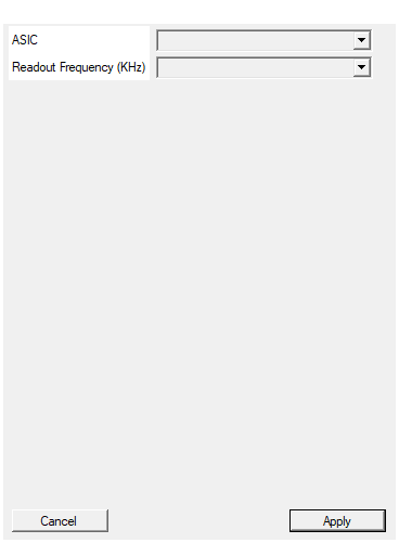
Select the ASIC to be connected to the Endpoint
Selects which of the four CITIROC 1A chips on the board this instance drives. It
does not change any pin; it renames the internal board nets the block binds to
(Citiroc_<ASIC>_ADC_ENERGY_HG/LG, Citiroc_<ASIC>_CHARGE_HIT_s,
Citiroc_<ASIC>_SRIN_s, Citiroc_<ASIC>_SCLK_s, Citiroc_<ASIC>_RESET_READ_s,
<ASIC>_VAL_EVT_s, <ASIC>_RAZ_CHN_s, <ASIC>_HOLD_HG_s, <ASIC>_HOLD_LG_s).
| Value | ASIC |
|---|---|
A |
chip A |
B |
chip B |
C |
chip C |
D |
chip D |
Two instances must never carry the same value — they would both drive the same
SCLK / HOLD nets.
This property is flagged isVisible = False in the component definition, so it is
not shown in the standard property dialog.
Default: A
Default: A
Options: A B C D
Set the readout frequency for the chip. Value higher than 500KHz reduce the quality of the measure
Nominal ASIC readout frequency in kHz. It sets the only generic of the instantiated
entity: CLKDIV = 160000 / ReadoutFrequency, and one shift-register step costs
2·(CLKDIV+1) global-clock cycles.
| Value (kHz) | CLKDIV |
|---|---|
| 1 | 160000 |
| 10 | 16000 |
| 50 | 3200 |
| 100 | 1600 |
| 200 | 800 |
| 400 | 400 |
| 500 | 320 |
| 1000 | 160 |
| 2500 | 64 |
| 4000 | 40 |
| 5000 | 32 |
Per the property description in the component, values above 500 kHz degrade the
quality of the measurement. Note that the constant 160000 is hard-coded in
CompileHDL: the project global clock frequency is read into a local variable but
is not used, so changing the design clock does not change CLKDIV.
This property is flagged isVisible = False in the component definition, so it is
not shown in the standard property dialog.
Default: 500
Default: 500
Options: 1 10 50 100 200 400 500 1000 2500 4000 5000
⚙️ Detailed Operation
Emitted HDL
CompileHDL writes the embedded resource CitirocAnalogReadout.vhd
(entity CITIROCAnalogReadout) to pcores/CitirocAnalogReadout.vhd and instantiates
it with a single generic:
| Generic | Value written by the compiler |
|---|---|
CLKDIV |
160000 / ReadoutFrequency (integer division, ReadoutFrequency in kHz) |
The entity also declares a TRIGGER_HOLD_DELAY generic and a CHIP_TEMP output port;
neither is driven or mapped by the compiler. TRIGGER_HOLD_DELAY keeps its VHDL
default and is dead code — the hold delay comes from the HOLD_TIME pin, not
from the generic.
Readout state machine
TRIG ↑
│
▼
[0] idle ──► [1] wait HOLD_TIME ──► [2] SR reset low ──► [3] 5 clk ──► [4][5] ──►
[6] first SCLK edge ──► ┌─► [7] SCLK low (CLKDIV+1 clk) ─┐
│ │ 35 slots
└── [8] SCLK high (CLKDIV+1 clk) ◄─┘ (sample here)
│ slot 34
▼
[9] publish outputs ──► [A] RAZ_CHN pulse ──► [B] dead time ──► [0]
TRIGis edge sensitive: the machine leaves idle on a0 → 1transition only. WhileTRIGstays high in idle,RAZ_CHNis held asserted (continuous channel reset).- Each shift-register step takes
2·(CLKDIV+1)clock cycles (states 7 and 8), so the shift clock produced onSCLKis $f_{\mathrm{SCLK}} = f_{\mathrm{clk}} / \left(2,(\mathrm{CLKDIV}+1)\right)$. - At each step the current filtered HG/LG pair and
CHARGE_HITare latched into an internal 35-entry buffer.
The 35 shift-register slots
The ASIC shift register is longer than the 32 channels. The FSM walks 35 slots and treats them differently:
Slot I |
Meaning | Where it goes |
|---|---|---|
| 0 … 31 | channel 0 … 31 | serial stream (S_*), parallel pins, frame word |
| 32 | chip temperature | internal CHIP_TEMP port only |
| 33 | dummy cycle | discarded |
| 34 | last step, exits the loop | discarded |
Serial output (S_*)
During slots 0…31 the block emits one word per channel:
S_DV is a single-cycle pulse; S_CHID (5 bit) says which channel the word belongs to.
S_HIT is the ASIC CHARGE_HIT discriminator state sampled at the same instant.
Parallel output (P_*) and the packed frame
When the last slot has been read, state 9 publishes everything at once:
- the 32
P_E_HG_n/P_E_LG_n/P_H_ntriplets, with a one-cycleP_DVpulse; - the 1024-bit
P_FRAME_DATAbus, withP_FRAME_DVraised and held.
P_FRAME_DATA is 32 concatenated 32-bit channel words. Channel 0 occupies the
most significant word (bits 1023:992) and channel 31 the least significant
(bits 31:0). Each 32-bit word is:
| Bits | Field | Width |
|---|---|---|
| 31:29 | "000" (reserved, always zero) |
3 |
| 28 | HIT — the channel discriminator |
1 |
| 27:14 | LG charge | 14 |
| 13:0 | HG charge | 14 |
Frame handshake
P_FRAME_DV is level, not a pulse. It goes high in state 9 and is cleared only
when P_FRAME_ACK is seen high:
This is what lets the round-robin arbiter inside Citiroc Frame Transfer poll the
four ASICs one after the other without losing an event. If P_FRAME_ACK is left
unconnected, P_FRAME_DV stays high forever after the first event.
Timestamps
TS_IN (64 bit) and TS0_IN (32 bit) are simply latched and forwarded to
TS_OUT / TS0_OUT at the instant the trigger edge is accepted. The block does not
generate or increment them — it only freezes the free-running counters that feed it,
so that the timestamp travelling with the event is the trigger time, not the
end-of-readout time.
Abort: REJECT
REJECT is tested every clock cycle, in every state. When it is high the FSM jumps
straight to the ASIC-reset state and restarts the RAZ_CHN sequence. No P_DV,
no P_FRAME_DV and no further S_DV are produced for that event — the event is
discarded in flight. Use it with a pile-up or veto detector to kill a bad event before
paying the full readout dead time.
Dead time
The dominant term is the shift-register walk:
$$ T_{\mathrm{dead}} ;\approx; \mathrm{HOLD_TIME} ;+; 35 \cdot 2,(\mathrm{CLKDIV}+1) ;+; \mathcal{O}(50) ;; \text{clock cycles} $$
With the default ReadoutFrequency = 500 (so CLKDIV = 320) on the 160 MHz global
clock of the DT5550W-Citiroc1A this is about 22 500 clocks ≈ 140 µs per event, and
the shift clock actually produced is $160,\mathrm{MHz}/642 \approx 249$ kHz.
Monitor outputs
M_ENERGY_HG / M_ENERGY_LG are the continuous output of the boxcar filter — they
are not gated by the readout and are live at all times. M_CLK and M_DIN mirror the
SCLK and SR_IN wires the block drives into the ASIC. All four are intended for a
logic analyser or an oscilloscope block, to debug the readout sequence without probing
the hardware.
Typical wiring
Citiroc Trigger ──TRIG──►┌──────────────────┐──P_FRAME_DATA──►┌────────────────┐
Timestamp ct. ──TS_IN───►│ Citiroc Analog │──P_FRAME_DV────►│ Citiroc Frame │──► PC
──TS0_IN──►│ (ASIC A) │◄─P_FRAME_ACK────│ Transfer │
pile-up det. ──REJECT──►│ │──TS_OUT/TS0_OUT►│ │
constant ─HOLD_TIME►└──────────────────┘ └────────────────┘
One instance per ASIC; set the ASIC property of each instance to A, B, C, D so that
each one binds to its own set of Citiroc_<ASIC>_* board nets.
Resources & Timing
-
Latency: Trigger edge to
P_DV≈ HOLD_TIME + 35·2·(CLKDIV+1) clock cycles (≈140 µs at the default 500 kHz setting on a 160 MHz clock) -
Throughput: One event per readout cycle;
BUSYis high for the whole cycle and no new trigger is accepted while it is high
- Emits
pcores/CitirocAnalogReadout.vhd(entityCITIROCAnalogReadout), the plainCitirocAnalogReadout.vhdresource — not the_NEWvariant, which belongs to the V2 block. - No memory-mapped registers and no SDK code:
CompileMMCandCompileSDKare empty. Everything software-visible comes from the downstream Citiroc Frame Transfer block. - 32-tap boxcar on both ADC inputs, truncated (no rounding); 24-bit accumulator, result taken from bits [20:5].
- The chip temperature is digitised at shift-register slot 32 but is not reachable from any pin.
- Supported board: DT5550W-Citiroc1A (
97567308-DA16-4E48-BB5E-ACE3E84DF06D). Not available inside subpages or state machines.