
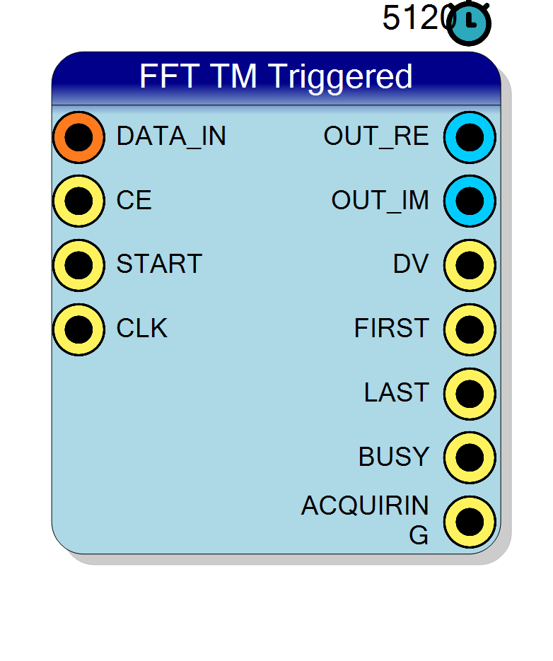
FFT TM Triggered
Triggered Fast Fourier Transform for Time-Multiplexed (TM) input signals. Accepts multiple samples per clock cycle (TM factor 2, 4, 8, or 16), accumulates a full frame into Block RAM on trigger, then computes the FFT and outputs sequential frequency-domain bins. The FFT starts consuming the buffer WHILE it is still filling, so the spectrum is ready as early as possible. Supports transform lengths from 128 to 16384 points, four engine architectures (Pipelined, Radix-4, Radix-2, Radix-2 Lite) with different area/speed trade-offs, 16-bit input and unscaled 32-bit complex output.
Introduction
The block computes the Fast Fourier Transform of a Time-Multiplexed (TM) input signal. TM signals carry multiple samples per clock cycle, enabling acquisition rates higher than the FPGA clock frequency. For example, with TM=4 at 125 MHz clock, the effective sampling rate is 500 MSps.
On a rising edge of START, the block begins accumulating TM input
samples into an internal Block RAM ($N / \text{TM}$ clock cycles, one
TM word per clock). While the buffer is still filling, a reader
already streams the stored samples to a standard Xilinx FFT core in
temporal order, one sample per clock: the reader consumes TM times
slower than the writer fills, so it can never overtake it. The core
then produces the sequential frequency-domain output burst.
$$ X[k] = \sum_{n=0}^{N-1} x[n] \cdot e^{-j2\pi kn/N}, \quad k = 0, 1, \ldots, N-1 $$
where $N$ is the FFT Length property, and $x[n]$ are the time-ordered samples extracted from the TM input bus.
The output is sequential (one bin per clock), not TM. This makes the block ideal for spectral analysis where the full spectrum is read out after each trigger event.
Pin Description
CE = 1 during the acquisition
phase ($N / \text{TM}$ clocks after START).
CE = 0, the acquisition phase pauses (samples are not stored).
Default connection: '1' (always enabled).
BUSY = 1
are ignored.
DV = 1. Outputs are produced sequentially in
natural order (bin 0, 1, 2, …, $N-1$).
DV = 1. For real-only input, $X[0]$ and $X[N/2]$
have zero imaginary parts.
OUT_RE and OUT_IM.
OUT_RE / OUT_IM.
BUSY goes low.
START until the last output bin has been produced.
Do not start a new transform while BUSY = 1.
Properties
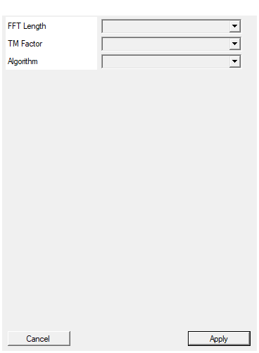
Number of points in the FFT transform (must be power of 2)
FFT transform length $N$ (number of points). Allowed values: 128, 256, 512, 1024, 2048, 4096, 8192, 16384. Larger transforms provide finer frequency resolution: $$ \Delta f = \frac{f_s}{N} = \frac{f_{\text{clk}} \times \text{TM}}{N} $$ Must be a multiple of the TM factor. Changing this value re-generates the underlying FFT IP core and adjusts the Block RAM depth.Default: 4096
Options: 128 256 512 1024 2048 4096 8192 16384
Time Multiplexing factor (number of samples per clock cycle)
Time Multiplexing factor (Super Sample Rate). Allowed values: 2, 4, 8, 16. Defines the number of samples carried on the input bus per clock cycle. The effective sampling rate is: $$ f_s = f_{\text{clk}} \times \text{TM} $$ The acquisition phase lasts $N / \text{TM}$ clock cycles. Higher TM factors reduce acquisition time but increase bus width and Block RAM usage.Default: 4
Options: 2 4 8 16
xfft engine. Pipelined Streaming: fastest, largest (can re-trigger back to back). Radix-4 Burst: ~4x smaller, transform ~(N/4)*log4(N) clocks. Radix-2 Burst: smaller again, ~(N/2)log2(N) clocks. Radix-2 Lite: smallest (time-shared butterfly), ~Nlog2(N) clocks.
Selects the FFT algorithm architecture:
- Pipelined: highest throughput (output follows the feed directly), largest area. Choose for maximum trigger rate.
- Radix-4: one radix-4 engine, transform in about $(N/4)\log_4 N$ clocks. Recommended default.
- Radix-2: one butterfly, about $(N/2)\log_2 N$ clocks, roughly a third of the DSPs of Radix-4.
- Radix-2 Lite: time-shared butterfly, about $N\log_2 N$ clocks, smallest possible footprint.
See the area/speed table in the description for concrete numbers.
Default: Radix-4
Options: Pipelined Radix-4 Radix-2 Radix-2 Lite
Functional description
The component performs three phases of operation:
Phase 1 — Acquisition (COLLECT)
After START rises, the block writes the incoming TM data bus into a
Block RAM (XPM SDPRAM). Each clock cycle stores one TM-wide word
containing $\text{TM}$ samples. This phase lasts $N / \text{TM}$ clock
cycles. During this phase, ACQUIRING is high.
TM bit ordering: The LSB of the TM bus contains the oldest sample (phase 0) and the MSB contains the newest sample (phase $\text{TM}-1$). This matches the standard SciCompiler TM convention.
Phase 2 — FFT feed (overlapped with the acquisition)
A reader streams the stored samples to the Xilinx FFT core in temporal order (lane 0 of word 0 first, then lane 1, …, lane $\text{TM}-1$, then word 1, and so on), one sample per clock. The feed starts as soon as the FIRST word has been captured - it runs concurrently with the acquisition, removing the wait-for-capture penalty of $N/\text{TM}$ clocks. Word availability is checked explicitly (a CE-gated pause of the capture simply stalls the reader) and the AXIS handshake with the core is honored - mandatory for the burst engines, which stop accepting input while they compute.
Phase 3 — Output (WAIT_OUTPUT)
The FFT IP core produces $N$ complex output bins in natural order
($k = 0, 1, \ldots, N-1$). Each bin is output on OUT_RE and OUT_IM
for one clock cycle with DV = 1.
DFT definition
$$ X[k] = \sum_{n=0}^{N-1} x[n] \cdot e^{-j2\pi kn/N} $$
where:
- $x[n]$ → time-domain input samples from the TM bus
- $X[k]$ → frequency-domain output as
OUT_RE[k] + j \cdot OUT_IM[k] - $N$ → transform length (128, 256, …, 16384)
Input and Output
Input: TM bus of 16-bit signed fixed-point samples. The bus width is $16 \times \text{TM}$ bits. Real data only (imaginary part assumed zero).
Output: 32-bit signed sequential complex bins, unscaled (full precision): the true magnitude grows to $16 + \log_2 N + 1$ bits (e.g. 27 bits for $N=1024$, 31 bits for $N=16384$), sign-extended to 32. No overflow is possible and no scaling schedule is needed:
OUT_RE: Real part of $X[k]$OUT_IM: Imaginary part of $X[k]$
Frequency resolution
The frequency resolution of the FFT output is:
$$ \Delta f = \frac{f_s}{N} = \frac{f_{\text{clk}} \times \text{TM}}{N} $$
For example, with $f_{\text{clk}} = 125,\text{MHz}$, $\text{TM} = 4$, $N = 4096$:
$$ \Delta f = \frac{500,\text{MHz}}{4096} \approx 122,\text{kHz} $$
Choosing the Algorithm : area vs speed
All four engines compute the same $N$-point transform; they differ in how much hardware is instantiated and therefore in how many clocks the transform takes. Approximate figures for 16-bit input (DSP counts grow mildly with $N$ through the twiddle stages):
| Algorithm | Area (DSP / memory) | Transform time (clocks) | When to use |
|---|---|---|---|
| Pipelined | largest: $\approx \log_4 N$ parallel stages, ~20-40 DSP, most BRAM | hidden: output follows the feed after $\approx N$ + pipeline latency | fastest repetition rate, back-to-back triggers |
| Radix-4 | one radix-4 engine, ~9-12 DSP | $\approx \tfrac{N}{4}\log_4 N$ | recommended default, good balance |
| Radix-2 | one radix-2 butterfly, ~3-4 DSP | $\approx \tfrac{N}{2}\log_2 N$ | area-constrained designs |
| Radix-2 Lite | time-shared butterfly, ~2-3 DSP, least logic | $\approx N\log_2 N$ | smallest possible footprint, speed irrelevant |
The burst engines (Radix-4 / Radix-2 / Radix-2 Lite) cannot accept new input while transforming, so the trigger-to-spectrum time is feed ($N$) + transform + unload ($N$). The Pipelined engine overlaps everything and is limited essentially by the feed alone.
Timing
The acquisition adds nothing to the latency: the reader trails the writer inside the same window. Measured in simulation ($N = 1024$, TM = 4, Radix-4, xsim): 3462 clocks from the START edge to the LAST output bin = feed 1024 + transform ~1400 + unload 1024. The same configuration with Pipelined completes in ~2200 clocks, Radix-2 in ~7200, Radix-2 Lite in ~12300 (from the cycle formulas above).
For a 4096-point FFT with TM=4 and Radix-4:
- acquisition: 1024 clocks (hidden under the feed)
- feed: 4096 clocks, starts ~3 clocks after START
- transform: ~6300 clocks
- unload: 4096 clocks
- Total: ~14500 clocks (~116 us at 125 MHz)
Block RAM usage
The acquisition buffer uses one XPM Simple Dual Port RAM:
- Depth: $N / \text{TM}$ words
- Width: $16 \times \text{TM}$ bits
- Example: 4096 points, TM=4 → 1024 x 64-bit = 8 KB (4 BRAM18)
Additional BRAM is used internally by the Xilinx FFT IP core.
Typical use cases
- Spectrum analysis of high-speed digitizer signals (>250 MSps)
- Triggered spectral measurements in nuclear/particle physics
- Post-trigger frequency analysis in radar/sonar systems
- Burst-mode spectrum analysis synchronized to external events
- Spectral monitoring of RF signals with TM-based ADC interfaces
Waveform example
Simplified timing for a 16-point FFT with TM=4:
Note: ACQUIRING is high only during the COLLECT phase.
BUSY remains high until all output bins have been produced.