
Logic Analyzer
Digital oscilloscope for FPGA signals. Captures multiple digital traces simultaneously with configurable trigger modes (software, external, edge detection). Ideal for debugging and signal analysis in real-time.
Introduction
Principle of Operation
The Logic Analyzer block is a digital oscilloscope that captures multiple digital signals simultaneously and stores them in a circular buffer for later readout. It is an essential debugging tool for analyzing timing relationships between FPGA signals.
Key Features
- Multiple traces: Capture multiple digital signals (buses) simultaneously
- Configurable depth: 256 to 65536 samples per capture
- Three trigger modes: Software, External, or Edge detection
- Pre-trigger data: 64 samples of pre-trigger history are always captured
- Real-time visualization: Integrated viewer in Resource Explorer
The Logic Analyzer data can be read via Resource Explorer or programmatically using the SciSDK library.
SciSDK Documentation: https://nuclearinstruments.github.io/SCISDK/
Pin Description
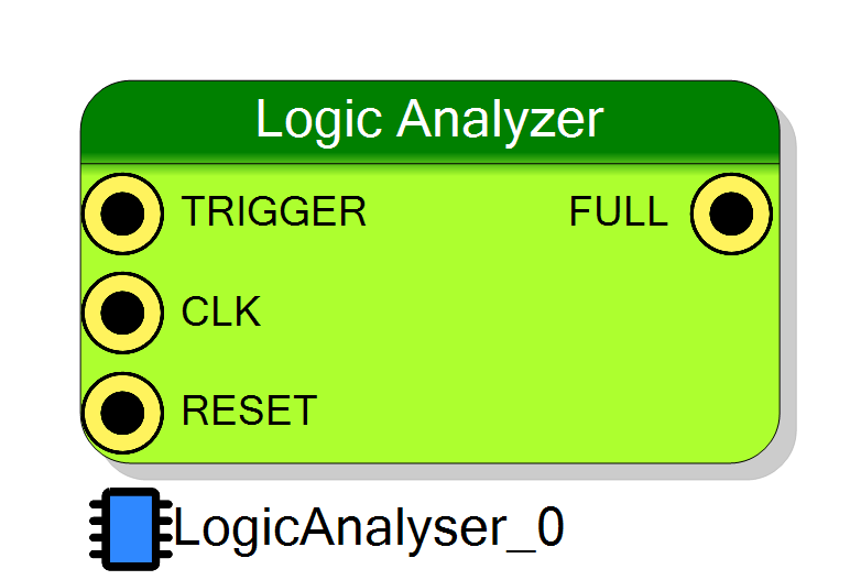
Trigger Input – External trigger signal.
When External trigger mode is enabled (CONFIG[2] = 1), acquisition starts when this signal goes HIGH.
Leave unconnected if using Software or Edge trigger modes.
Clock – Sampling clock for data capture.
All signals are sampled on the rising edge of this clock. Default: CLK_ACQ (80 MHz on DT5560/DT5550).
Full – HIGH when the capture buffer is full.
This signal indicates that the acquisition is complete and data is ready to be read.
Data Input – Digital signals to be captured.
This is a multi-pin input that can be expanded to connect multiple signals. Each connected signal becomes a separate trace in the Logic Analyzer.
The total bit width determines the FPGA resources used.
Properties
Set the name of the endpoint
Logical endpoint name used in register map. Used in Resource Explorer and SciSDK. Default: LogicAnalyser_0Default: LogicAnalyser_0
Set the number of samples stored
Number of samples to capture per acquisition. Available values: 256, 512, 1024, 2048, 4096, 8192, 16384, 32768, 65536.
More samples provide longer capture time but use more FPGA memory. Default: 1024
Default: 1024
Options: 256 512 1024 2048 4096 8192 16384 32768 65536
JSON Array with interface definition
JSON configuration defining the input buses and their properties.
This is configured through the graphical editor when creating the block. Each bus entry specifies:
- Name (displayed in Resource Explorer)
- Bit width
Detailed Operation
Data Flow
┌──────────────────────────────────────────────────────────────────────┐
│ Logic Analyzer Data Flow │
│ │
│ BUS (N bits) ──────►┌──────────────┐ ┌─────────────┐ │
│ │ 64-sample │ │ │ │
│ │ Pre-Delay │────►│ FIFO │───► PC │
│ TRIGGER ───────────►│ │ │ Buffer │ │
│ │ Trigger │ │ │ │
│ CLK ───────────────►│ Logic │ │ │ │
│ └──────────────┘ └─────────────┘ │
│ RESET ──────────────────┘ │ │
│ ┌────┴────┐ │
│ │ FULL │──► HIGH when capture complete │
│ └─────────┘ │
└──────────────────────────────────────────────────────────────────────┘
State Machine
The Logic Analyzer operates with a simple 3-state machine:
┌─────────────────────────────────────────────────────────────────────┐
│ State Machine │
│ │
│ ┌──────┐ ARM rising ┌───────────────┐ │
│ │ IDLE │ ────────────────►│ WAIT_TRIGGER │ │
│ │ (0) │◄─────────────── │ (1) │ │
│ └──────┘ capture done └───────┬───────┘ │
│ ▲ │ │
│ │ trigger condition │
│ │ │ │
│ │ ▼ │
│ │ ┌───────────────┐ │
│ └─────────────────────│ CAPTURE │ │
│ buffer full │ (2) │ │
│ └───────────────┘ │
└─────────────────────────────────────────────────────────────────────┘
State descriptions:
| State | Description | Status Bits |
|---|---|---|
| IDLE (0) | Waiting for ARM command | RM=0, RMA=0 |
| WAIT_TRIGGER (1) | Armed, waiting for trigger | RM=1, RMA=1 |
| CAPTURE (2) | Trigger occurred, filling buffer | RM=0, RMA=1 |
Trigger Modes
The Logic Analyzer supports three trigger modes:
| Mode | CONFIG Bit | Description |
|---|---|---|
| External | CONFIG[2] = 1 | Triggers when TRIGGER input goes HIGH |
| Edge | CONFIG[3] = 1 | Triggers on rising/falling edge of any bus bit |
| Software | CONFIG[4] = 1 | Free-running, starts immediately after ARM |
Edge Trigger Configuration
When using edge trigger mode (CONFIG[3] = 1), you can configure which bits trigger on rising edge, falling edge, or both:
| Registers | Function |
|---|---|
| CONFIG0-CONFIG7 | Rising edge enable mask (256 bits total) |
| CONFIG8-CONFIGF | Falling edge enable mask (256 bits total) |
Each bit in these registers corresponds to a bit position in the input BUS. Setting a bit to 1 enables triggering on that edge type.
Example: To trigger on rising edge of bit 0 and falling edge of bit 5:
- Set CONFIG0 = 0x00000001 (rising edge on bit 0)
- Set CONFIG8 = 0x00000020 (falling edge on bit 5)
Pre-Trigger Delay
The Logic Analyzer includes a 64-sample delay line that ensures 64 samples of pre-trigger data are always captured. This allows you to see what happened before the trigger event.
Timing Diagram - Software Trigger
Timing Diagram - External Trigger
Timing Diagram - Edge Trigger
Configuration Registers
CONFIG
| Bit | Function |
|---|---|
| 0 | ARM (rising edge starts acquisition) |
| 1 | Reset |
| 2 | External trigger enable |
| 3 | Edge trigger enable |
| 4 | Software trigger (free-running) |
CONFIG0 - CONFIG7
Rising edge trigger enable mask. Each register is 32 bits, providing 256 bits total. Setting bit N to 1 enables rising edge detection on input bus bit N.
CONFIG8 - CONFIGF
Falling edge trigger enable mask. Each register is 32 bits, providing 256 bits total. Setting bit N to 1 enables falling edge detection on input bus bit N.
STATUS
| Bits | Function |
|---|---|
| 0 | flag_captured (1 = capture complete) |
| 1 | RM (1 = waiting for trigger) |
| 2 | RMA (1 = armed/running) |
| 31:8 | Read words available in FIFO |
Software Integration with SciSDK
The Logic Analyzer is fully supported by SciSDK.
Available Parameters
| Parameter | Access | Description | Default |
|---|---|---|---|
trigger_mode |
R/W | software, external, or edge |
software |
acq_mode |
R/W | blocking or non-blocking |
blocking |
timeout |
R/W | Timeout in ms for blocking mode | 1000 |
trigger_rising_mask |
R/W | Rising edge mask (string of 0/1) | “0…0” |
trigger_falling_mask |
R/W | Falling edge mask (string of 0/1) | “0…0” |
ntraces |
R | Number of digital traces | (from design) |
nsamples |
R | Number of samples | (from design) |
Available Commands
| Command | Description |
|---|---|
start |
Reset, configure trigger, and arm the analyzer |
reset |
Reset the analyzer and stop acquisition |
Buffer Structure
c
typedef struct {
uint32_t magic; // Buffer type identifier
uint32_t timecode; // Acquisition timestamp (microseconds)
uint32_t *data; // Pointer to sample data
struct {
uint32_t samples; // Number of samples captured
uint32_t ntraces; // Number of digital traces
uint32_t words_per_sample; // 32-bit words per sample
} info;
} SCISDK_LOGICANALYSER_DECODED_BUFFER;
Data organization: Each sample consists of words_per_sample 32-bit words.
The traces are packed bit-by-bit into these words.
C/C++ Example
c
#include "SciSDK_DLL.h"
// Allocate buffer
SCISDK_LOGICANALYSER_DECODED_BUFFER *buffer;
SCISDK_AllocateBuffer("board0:/MMCComponents/LogicAnalyser_0",
T_BUFFER_TYPE_DECODED,
(void**)&buffer, _sdk);
// Configure: external trigger, blocking mode
SCISDK_SetParameterString("board0:/MMCComponents/LogicAnalyser_0.trigger_mode",
"external", _sdk);
SCISDK_SetParameterString("board0:/MMCComponents/LogicAnalyser_0.acq_mode",
"blocking", _sdk);
SCISDK_SetParameterInteger("board0:/MMCComponents/LogicAnalyser_0.timeout",
5000, _sdk); // 5 seconds
// Start acquisition
SCISDK_ExecuteCommand("board0:/MMCComponents/LogicAnalyser_0.start", "", _sdk);
// Read data (blocks until trigger or timeout)
int ret = SCISDK_ReadData("board0:/MMCComponents/LogicAnalyser_0",
(void*)buffer, _sdk);
if (ret == NI_OK) {
printf("Captured %d samples, %d traces\n",
buffer->info.samples, buffer->info.ntraces);
// Extract trace 0 data
for (int s = 0; s < buffer->info.samples; s++) {
int word_idx = s * buffer->info.words_per_sample;
uint32_t trace0_value = buffer->data[word_idx] & 0x01;
printf("Sample %d: trace0 = %d\n", s, trace0_value);
}
}
// Free buffer
SCISDK_FreeBuffer("board0:/MMCComponents/LogicAnalyser_0",
T_BUFFER_TYPE_DECODED, (void**)&buffer, _sdk);
Python Example
python
from scisdk.scisdk import SciSDK
import matplotlib.pyplot as plt
sdk = SciSDK()
sdk.AddNewDevice("usb:10500", "dt5560", "board0", "RegisterFile.json")
# Allocate buffer
res, buf = sdk.AllocateBuffer("board0:/MMCComponents/LogicAnalyser_0",
sdk.T_BUFFER_TYPE_DECODED)
# Configure: edge trigger on trace 0 rising edge
sdk.SetParameter("board0:/MMCComponents/LogicAnalyser_0.trigger_mode", "edge")
sdk.SetParameter("board0:/MMCComponents/LogicAnalyser_0.trigger_rising_mask", "1")
sdk.SetParameter("board0:/MMCComponents/LogicAnalyser_0.acq_mode", "blocking")
sdk.SetParameter("board0:/MMCComponents/LogicAnalyser_0.timeout", 5000)
# Start and wait for trigger
sdk.ExecuteCommand("board0:/MMCComponents/LogicAnalyser_0.start", "")
res, buf = sdk.ReadData("board0:/MMCComponents/LogicAnalyser_0", buf)
if res == 0:
nsamples = buf.info.samples
ntraces = buf.info.ntraces
words_per_sample = buf.info.words_per_sample
# Extract traces
traces = []
for t in range(ntraces):
word_offset = t // 32
bit_offset = t % 32
trace_data = []
for s in range(nsamples):
word_idx = s * words_per_sample + word_offset
bit_value = (buf.data[word_idx] >> bit_offset) & 1
trace_data.append(bit_value)
traces.append(trace_data)
# Plot traces
fig, axes = plt.subplots(ntraces, 1, figsize=(12, 2*ntraces), sharex=True)
for i, (ax, trace) in enumerate(zip(axes if ntraces > 1 else [axes], traces)):
ax.step(range(nsamples), trace, where='post')
ax.set_ylabel(f'Trace {i}')
ax.set_ylim(-0.1, 1.1)
ax.grid(True, alpha=0.3)
axes[-1].set_xlabel('Sample')
plt.tight_layout()
plt.show()
sdk.ExecuteCommand("board0:/MMCComponents/LogicAnalyser_0.reset", "")
Resource Explorer
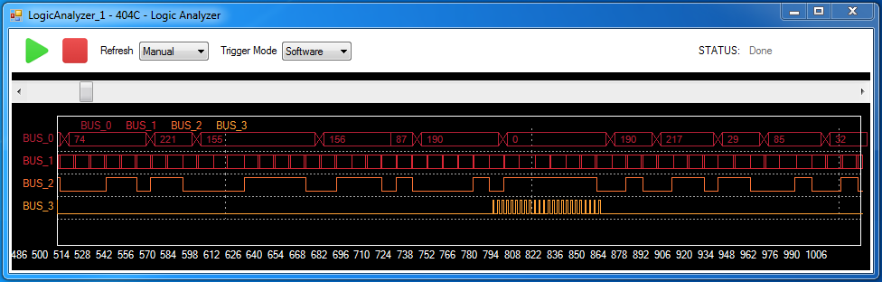
The Logic Analyzer tool in Resource Explorer provides real-time waveform visualization with zoom capabilities and multiple display modes for digital signals.
Display Features
- 1-bit signals: Displayed as digital waveforms (high/low)
- Multi-bit buses: Displayed as value blocks with transition markers
- Zoom: Use mouse wheel to zoom in/out on the time axis
- Pan: Use the horizontal scrollbar to navigate through the capture
Quick Reference
| Item | Description |
|---|---|
| Buffer depth | 256 to 65536 samples |
| Pre-trigger | 64 samples |
| Trigger modes | Software, External, Edge |
| Edge detection | Rising, Falling, or Both |
| Best for | Signal debugging, timing analysis |
Resources & Timing
-
Latency: 64 clock cycles pre-trigger delay
-
Throughput: One sample per clock cycle
- Uses BRAM for sample storage
- Dual-clock FIFO for clock domain crossing
- 64-sample pre-trigger delay line
- Supports buses up to 256 bits total
- Edge detection on any input bit