
Gate & Delay (Hardware)
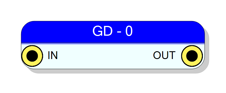
Hardware Gate & Delay generator for V2495. Provides precise timing control with picosecond-resolution delay and gate width adjustment using a ring oscillator.
Introduction
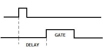
The Gate & Delay (Hardware) block interfaces with the V2495’s built-in precision timing system. It generates a fixed-width pulse at a precise delay from the rising edge of an input signal.
The V2495 implements 32 independent Gate & Delay channels with picosecond resolution.
Pin Description
Properties
Gate And Delay Port
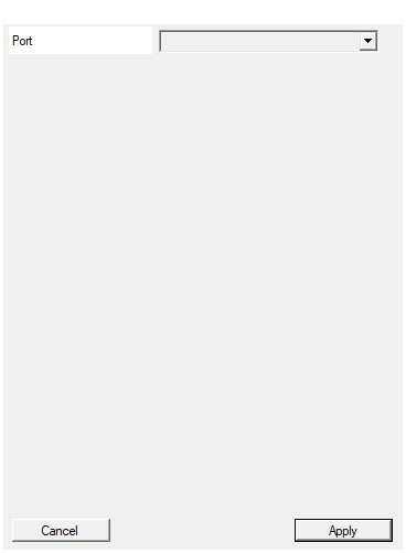
Gate & Delay port number (0-31). The V2495 has 32 independent Gate & Delay channels. Select the port that corresponds to your timing requirements.Default: 0
Options: 0 1 2 3 4 5 6 7 8 9 10 11 12 13 14 15 16 17 18 19 20 21 22 23 24 25 26 27 28 29 30 31
Usage
How It Works
The Gate & Delay system generates a delayed pulse from an input trigger:
┌──────────────────────────────────────────────────────────────────┐
│ Gate & Delay Timing │
│ │
│ INPUT: ──┐ ┌────────────── │
│ └─────┘ │
│ │
│ ◄──────► DELAY │
│ │
│ OUTPUT: ────────────┐ ┌────────────── │
│ └─────────┘ │
│ ◄─────────► │
│ GATE │
└──────────────────────────────────────────────────────────────────┘
Ring Oscillator Implementation
The Gate & Delay is implemented using a ring oscillator inside the FPGA. The frequency of the ring oscillator can be controlled by setting the FINE value.
| Parameter | Description | Range |
|---|---|---|
| DELAY | Delay from input rising edge | 0-65535 |
| GATE | Output pulse width | 0-65535 |
| FINE | Fine timing adjustment | 1-255 |
Important: The FINE step depends on:
- FPGA manufacturing process
- Device temperature
- Individual channel characteristics
Calibration Procedure
Since FINE values are process/temperature dependent, calibration is recommended:
- Set GATE to 1000
- Provide a test pulse
- Set FINE to 1, measure output with oscilloscope
- Set FINE to 255, measure output with oscilloscope
- Calculate FINE step for this channel
This procedure is required only once per board.
Software Configuration
The Gate & Delay parameters are configured via the PC library:
c
// At application startup:
GateDelay_Reset_delay(handle);
GateDelay_Calibrate(handle);
// Program delay and gate:
GateDelay_Program(handle, channel, delay, gate, fine);
Maximum values: DELAY = 65535, GATE = 65535
Port Selection
The V2495 has 32 independent Gate & Delay channels (ports 0-31). Select the port number in the block properties to match your design.
Resources & Timing
-
Latency: Programmable delay (0-65535 units)
-
Throughput: Single-shot per trigger
- Picosecond-resolution timing
- Ring oscillator implementation
- Per-channel calibration recommended
- Configuration via PC software library
Supported Boards
- V2495