
Serial Bus - SPI Master
SPI Master controller for synchronous serial communication with configurable data width, multiple slave support, and full-duplex operation. Supports all four SPI modes via configurable clock polarity and phase.
Introduction
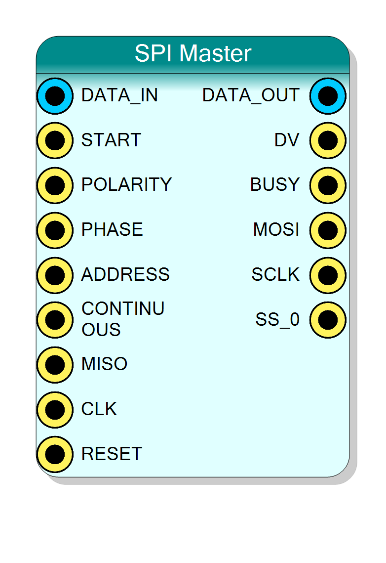
The SPI Master block implements a Serial Peripheral Interface master controller for synchronous full-duplex communication with one or more slave devices.
SPI uses four main signals:
- SCLK - Serial Clock (generated by master)
- MOSI - Master Out, Slave In (data from master to slave)
- MISO - Master In, Slave Out (data from slave to master)
- CS/SS - Chip Select / Slave Select (active low)
Key features:
- Configurable data width (1-32 bits)
- Support for up to 16 slave devices
- All four SPI modes supported (CPOL/CPHA combinations)
- Continuous mode for streaming data
- Programmable SCLK frequency
Pin Description
SPI clock polarity (CPOL).
- 0: SCLK is normally low (idle low)
- 1: SCLK is normally high (idle high)
SPI clock phase (CPHA).
- 0: Data sampled on first clock edge
- 1: Data sampled on second clock edge
Continuous mode enable.
- LOW: Complete transfer and deassert CS after data
- HIGH: Continue with next data word without releasing CS
Busy/Ready status output.
- LOW: Master is ready to accept commands
- HIGH: Transfer in progress
Properties
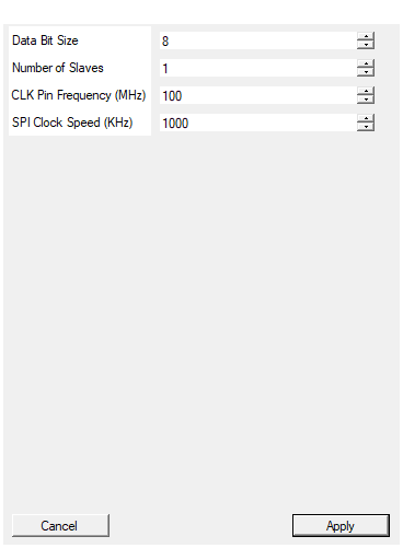
Set the number of bits for data transmission (1-32)
Default: 8
Range: 1 – 32
Set the number of SPI slave devices (1-16)
Default: 1
Range: 1 – 16
Set the input clock frequency in MHz
Default: 100
Range: 1 – 500
Set the desired SCLK frequency in KHz
Default: 1000
Range: 1 – 50000
Number of bits per data word (1-32). Determines the width of Data In and Data Out ports.
Common values:
- 8: Most common for byte-oriented devices
- 16: 16-bit ADCs, DACs
- 24: 24-bit ADCs
- 32: 32-bit registers
Number of slave devices (1-16). Creates one CS output for each slave.
The Address port width is automatically sized:
- 1 slave: 1-bit address
- 2-4 slaves: 2-bit address
- 5-8 slaves: 3-bit address
- 9-16 slaves: 4-bit address
Frequency of the CLK input in MHz. Used to calculate the clock divider for SCLK generation.
Typical values:
- 50 MHz: V2495 default
- 80 MHz: DT5550 default
- 100-200 MHz: High-speed designs
Desired SCLK frequency in KHz. Must be less than half the CLK frequency.
Common SPI speeds:
- 100-400 KHz: Slow devices, long cables
- 1-10 MHz: Most SPI devices
- 20-50 MHz: High-speed flash, ADCs
Actual frequency depends on CLK and may be slightly different from requested due to integer clock divider.
Functional description
The SPI Master generates the serial clock and controls data transmission with the selected slave device. Communication is full-duplex: data is simultaneously transmitted on MOSI and received on MISO.
SPI Clock Modes
The clock behavior is controlled by two parameters:
- CPOL (Clock Polarity): Idle state of SCLK
- CPHA (Clock Phase): Data sampling edge
| Mode | CPOL | CPHA | Description |
|---|---|---|---|
| 0 | 0 | 0 | SCLK idle low, sample on rising edge |
| 1 | 0 | 1 | SCLK idle low, sample on falling edge |
| 2 | 1 | 0 | SCLK idle high, sample on falling edge |
| 3 | 1 | 1 | SCLK idle high, sample on rising edge |
Master and slave must be configured for the same mode.
Transaction Flow
- Set Data In with data to transmit
- Set Polarity and Phase for desired SPI mode
- Set Address to select target slave (0 to NumSlaves-1)
- Set Continuous low for single transfer, high for streaming
- Pulse Start high to begin transaction
- Busy goes high during transfer
- When Busy goes low, DV pulses high
- Read received data from Data Out
Continuous Mode
When Continuous is high during the last bit of a transfer:
- The master latches new data from Data In
- Transmission continues without releasing CS
- DV pulses briefly to indicate received data is ready
- Useful for streaming multiple words without gaps
Clock Frequency
The SCLK frequency is calculated as:
$$ f_{SCLK} = \frac{f_{CLK}}{2 \times (clk_div + 1)} $$
The compiler automatically calculates the clock divider based on the configured CLK frequency and desired SPI speed.
Timing
- Busy asserts on the clock edge after Start is detected
- Data is valid when Busy goes low
- DV pulses for one clock cycle on falling edge of Busy
- In continuous mode, DV pulses after each word transfer
Reset Behavior
The Reset input is active low (active when ‘0’):
- All slave selects go high (deasserted)
- MOSI goes high-impedance
- Data Out clears to zero
- Busy goes high during reset, low when ready