Firmware Compilation
Complete guide to FPGA firmware compilation in SCI-Compiler. Learn the compilation process from VHDL generation through synthesis, implementation, and bitstream creation. Understand compiler output, troubleshoot errors, and use the Compile SDK feature for library generation.
Introduction
After designing your FPGA firmware with blocks and connections, the next step is compilation - transforming the graphical design into a bitstream file that can be programmed onto the FPGA.
Prerequisites
Before starting compilation, you must configure the paths to FPGA tools in the Settings window. See SCI-Compiler Configuration for details.
Required tools:
- Vivado (Xilinx) - For DT5550, DT1260, DT5550W boards
- Quartus (Intel/Altera) - For V2495, V2495X boards
Starting Compilation
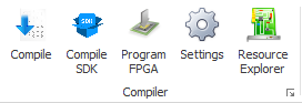
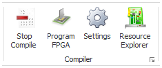
Figure 1: Compile button transforms to Stop Compilation during process
How to Compile
- Complete your block diagram design
- Connect all required inputs/outputs
- Configure memory mapping (if using MMC)
- Click Compile button in Home toolbar
During Compilation
Button changes:
- Compile → Stop Compilation (allows aborting)
Interface updates:
- Compiler Output tab displayed automatically
- Status bar shows “COMPILING”
- Progress bar animates

Figure 2: Status bar during compilation
Stop Compilation
To abort the compilation process:
- Click Stop Compilation button
- Current process terminates
- Button reverts to Compile
- Status returns to IDLE
Compilation Stages
The compilation process consists of multiple stages, each performing specific tasks.
Stage 1: VHDL Generation
Performed by: SCI-Compiler
Tasks:
- Generate register and signal mapping
- Assign unique names to blocks (U0, U1, U2…)
- Create HDL code for each block
- Generate VHDL files in
HDL/pcores/folder - Assemble all diagram files (main + sub-designs)
- Create top-level
.vhdfiles inHDL/folder
Output messages:
- Displayed in blue in Compiler Output
- Errors shown in red
Example messages:
Creating project structure...
Generating register map...
Processing block U0: Oscilloscope_0
Processing block U1: Leading_Edge_Trigger
Generating VHDL for main design...
VHDL generation complete.
Generated files:
HDL/pcores/- Individual block VHDL modulesHDL/design_1_wrapper.vhd- Top-level wrapperHDL/design_1.vhd- Main design
Stage 2: SDK and Library Generation
Performed by: SCI-Compiler
Tasks:
- Create C library for board communication
- Generate Python bindings
- Create example projects (VC++, gcc, Xcode compatible)
- Generate RegisterFile.json descriptor
Output location: library/ folder
Generated files:
C SDK:
NIDriver.c/h- Low-level driverNI_types.h- Type definitionsRegisterFile.json- Memory map descriptor- Example projects with makefiles
Python SDK:
scisdk.py- Python wrapper- Example scripts
RegisterFile.json: Contains all registers, oscilloscopes, lists, spectra, and logic analyzers for:
- Resource Explorer testing
- SDK function mapping
- Address lookup
Example RegisterFile.json:
json
{
"Device": "DT5550",
"Project": "my_design",
"Registers": [
{"Name": "threshold", "Address": 0, "RegionSize": 1}
],
"MMCComponents": [
{
"Name": "Oscilloscope_0",
"Type": "Oscilloscope",
"Address": 4096,
"channels": 4,
"samples": 1024
}
]
}
Stage 3: FPGA Synthesis and Implementation
Performed by: Vivado or Quartus (external tools)
Tasks:
- Generate TCL script in
HDL/folder - Launch Vivado/Quartus from shell
- Execute synthesis and implementation
Output:
- Redirected to Compiler Output
- Standard messages in black
- Warnings in orange
- Errors in red
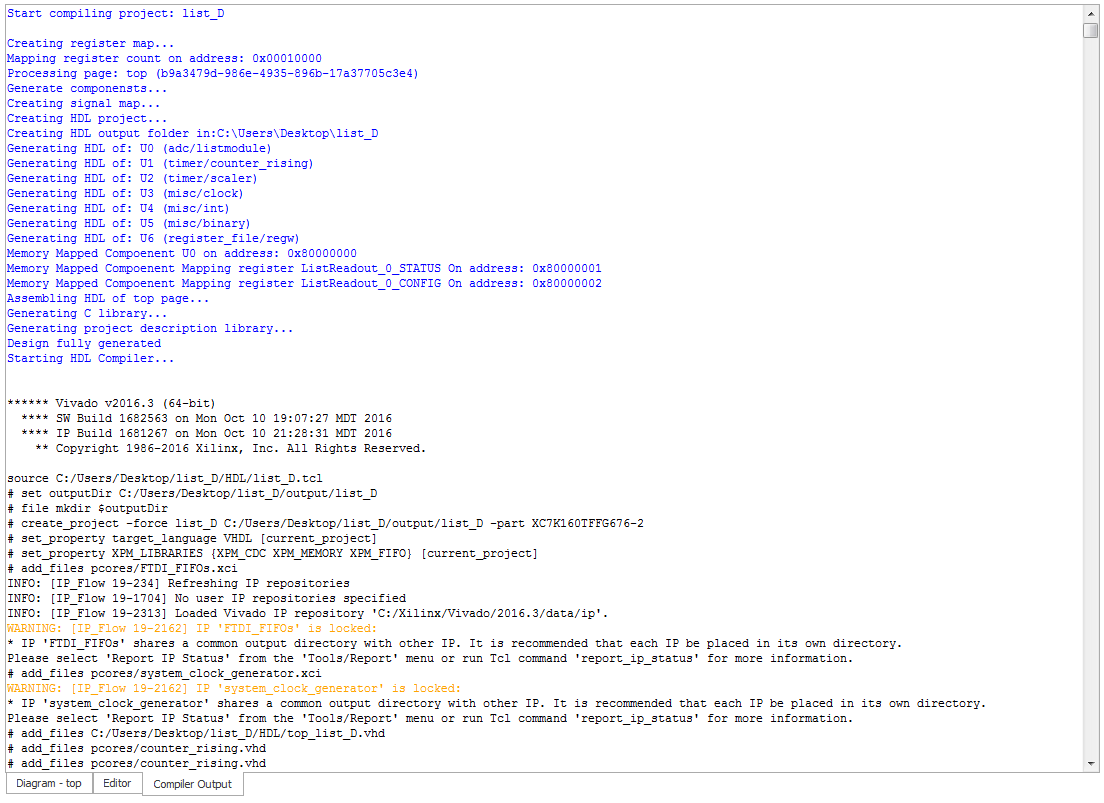
Figure 3: Vivado output in Compiler Output tab
Synthesis Phase
Purpose: Convert VHDL to gate-level netlist
Steps:
- Elaboration - Parse VHDL, check syntax
- RTL Synthesis - Convert behavioral to structural
- Optimization - Minimize logic, apply constraints
- Technology Mapping - Map to FPGA primitives
Typical messages:
Synthesis started...
Elaborating entity <design_1_wrapper>
Synthesizing module <design_1>
Synthesizing module <Oscilloscope_0>
Finished synthesis
Warnings to watch:
- Unused signals (may indicate wiring errors)
- Unconnected pins (check your diagram)
- Inferred latches (timing issues possible)
Implementation Phase
Purpose: Place and route synthesized design
Steps:
- Opt Design - Post-synthesis optimization
- Place Design - Assign gates to physical locations
- Route Design - Connect placed elements with wires
- Timing Analysis - Verify timing constraints met
Typical messages:
Starting implementation...
Opt_design started
Place_design started
Route_design started
Checking timing constraints...
Implementation complete
Critical warnings:
- Timing violations (design may not work reliably)
- Unroutable nets (resource conflicts)
- High fanout signals (performance impact)
Compilation Phases Summary
| Phase | Tool | Duration | Output |
|---|---|---|---|
| Analysis/Synthesis | Vivado/Quartus | 2-5 min | Netlist |
| Mapping | Vivado/Quartus | 1-3 min | Technology-mapped design |
| Place & Route | Vivado/Quartus | 5-15 min | Physical layout |
| Timing Analysis | Vivado/Quartus | 1-2 min | Timing report |
| Bitstream | Vivado/Quartus | 1-2 min | .bit/.rpd file |
Total compilation time: Typically 10-30 minutes, depending on design complexity.
Stage 4: Bitstream Generation
Purpose: Create configuration file for FPGA programming
Output files:
For DT5550/DT1260/DT5550W (Xilinx):
.bitfile - Binary bitstream- Location:
output/folder
For V2495/V2495X (Intel/Altera):
.rpdfile - Raw Programming Data- Location:
output/folder
Additional outputs:
.ltx- Logic analyzer probe file.dcp- Design checkpoint (Vivado)- Reports (timing, utilization, power)
Compilation Success
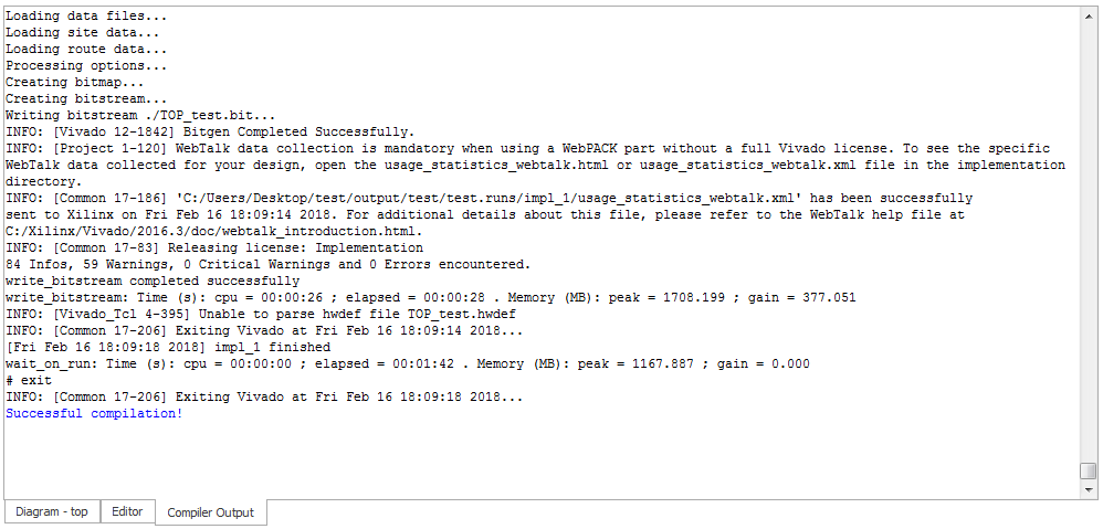
Figure 4: Successful compilation message
Success Indicators
Compiler Output message:
Successful compilation!
Status bar:
- Returns to IDLE
- Progress bar resets
Button:
- Stop Compilation → Compile
Generated files available:
- Bitstream in
output/folder - SDK library in
library/folder - RegisterFile.json for testing
- Ready to program FPGA!
Compilation Errors
If errors occur during compilation, the process stops.
Error Indicators
Compiler Output:
- Error messages in red
- Process halts at error point
Status bar:
- Returns to IDLE
- Progress bar resets
Button:
- Stop Compilation → Compile
Common Error Types
VHDL Generation Errors (Stage 1)
Unconnected required inputs:
ERROR: Block U5 (Oscilloscope_0) input 'DATA' is not connected
Solution: Connect all required input pins (usually IN, DATA, CLK)
Type mismatch:
ERROR: Cannot connect Integer output to Vector input
Solution: Use type conversion blocks or check connection logic
Duplicate names:
ERROR: Endpoint name 'Oscilloscope_0' already exists
Solution: Ensure all endpoint names are unique
Synthesis Errors (Stage 3)
Syntax errors in VHDL:
ERROR: Syntax error near line 234
Solution: Usually indicates SCI-Compiler bug - report to support
Undefined signals:
ERROR: Signal 'data_out' is not declared
Solution: Regenerate VHDL (clean build) or report bug
Resource overflow:
ERROR: Design exceeds available LUTs/BRAMs/DSPs
Solution: Simplify design, reduce buffer sizes, use fewer blocks
Implementation Errors (Stage 3)
Timing violations:
ERROR: Timing constraints not met (slack -2.345 ns)
Solution:
- Reduce clock frequency
- Simplify logic paths
- Add pipeline stages
Unroutable design:
ERROR: Unable to route all signals
Solution: Design too complex, reduce resource usage
Bitstream Generation Errors (Stage 4)
File I/O errors:
ERROR: Cannot write bitstream to output folder
Solution: Check disk space, folder permissions
Compile SDK Only
The Compile SDK button generates SDK library and examples without recompiling the entire FPGA design.
When to Use Compile SDK
Scenarios:
- Changed register descriptions (no functional change)
- Updated endpoint names (for documentation)
- Regenerate RegisterFile.json
- Update SDK without waiting for full compilation
What It Does
Generates:
- C/Python SDK library
- Example projects
- RegisterFile.json
Does NOT generate:
- VHDL code
- New bitstream
- FPGA configuration
Process
- Click Compile SDK button (next to Compile)
- Stage 2 executes only
- SDK files updated in
library/folder - Much faster than full compilation (~10 seconds)
Use case: You already have a working bitstream programmed on the board, but you want to regenerate SDK with updated comments or naming for your software development.
Compiler Output Messages
Understanding the color-coded messages:
Message Colors
| Color | Source | Meaning |
|---|---|---|
| Blue | SCI-Compiler | Internal operations (VHDL gen, SDK gen) |
| Black | Vivado/Quartus | Standard synthesis/implementation output |
| Orange | Vivado/Quartus | Warnings (non-critical issues) |
| Red | Any | Errors (compilation failure) |
Reading the Output
Progress indicators:
[10%] Generating VHDL...
[20%] Creating SDK...
[30%] Starting synthesis...
[50%] Optimization complete...
[70%] Placing design...
[90%] Routing complete...
[100%] Bitstream generated
Resource utilization:
Slice LUTs: 12345 / 63400 (19%)
Slice Registers: 8901 / 126800 (7%)
Block RAM: 45 / 135 (33%)
DSP Slices: 12 / 240 (5%)
Timing summary:
Worst Negative Slack: 0.234 ns (PASS)
Timing Errors: 0
Project Output Folders
After compilation, your project folder contains:
MyProject/
├── MyProject.scf # SCI-Compiler project file
├── MyProject.jpg # Diagram preview
├── HDL/ # Generated VHDL
│ ├── design_1.vhd
│ ├── design_1_wrapper.vhd
│ ├── pcores/ # Individual block VHDL
│ └── *.tcl # Vivado/Quartus scripts
├── library/ # SDK files
│ ├── NIDriver.c/h
│ ├── scisdk.py
│ ├── RegisterFile.json
│ └── examples/
└── output/ # Compilation outputs
├── design_1.bit/.rpd # Bitstream
├── *.rpt # Reports (timing, utilization)
└── *.ltx # Logic analyzer probes
Best Practices
Before Compilation
- Verify connections - All required inputs connected
- Check memory mapping - No address conflicts
- Review warnings - Fix any diagram issues
- Save project - Ctrl+S before compiling
During Compilation
- Monitor output - Watch for warnings in orange
- Don’t interrupt - Avoid stopping unless critical error
- Check timing - Note any timing violations
- Review resource usage - Ensure not exceeding limits
After Compilation
- Check “Successful compilation!” message
- Verify bitstream exists in
output/folder - Review timing reports - Ensure positive slack
- Test with Resource Explorer before custom software
Optimization Tips
Reduce compilation time:
- Use precompiled cores (if enabled)
- Minimize design changes between compilations
- Use Compile SDK for SDK-only updates
Improve timing:
- Reduce clock frequencies
- Add pipeline registers
- Minimize combinational logic depth
- Use registered outputs
Reduce resource usage:
- Minimize buffer sizes (oscilloscope, spectrum)
- Share resources between channels
- Use appropriate data widths (not always 32-bit)
- Remove unused blocks
Troubleshooting
Compilation Takes Too Long
Problem: Compilation exceeds 1 hour
Solutions:
- Check design complexity (too many blocks?)
- Verify Vivado/Quartus not stalled (check Task Manager)
- Increase compilation timeout in Settings
- Simplify design (reduce oscilloscope buffers, etc.)
Compilation Fails Immediately
Problem: Error in first few seconds
Solutions:
- Check Vivado/Quartus path in Settings
- Verify license for FPGA tools
- Ensure tools are installed correctly
- Check diagram for unconnected blocks
Bitstream Not Generated
Problem: Compilation reports success but no .bit/.rpd
Solutions:
- Check
output/folder manually - Review last 50 lines of Compiler Output
- Ensure disk space available
- Check folder permissions
Resource Overflow
Problem: “Exceeds available LUTs/BRAMs”
Solutions:
- Reduce oscilloscope samples (1024 → 512)
- Reduce spectrum bins (8192 → 4096)
- Remove unused channels
- Simplify processing algorithms
- Use precompiled cores if available
Timing Violations
Problem: “Timing constraints not met”
Solutions:
- Reduce system clock frequency
- Check critical paths in timing report
- Add pipeline stages to long paths
- Simplify complex combinational logic
- Contact support if persistent
Summary
Firmware compilation transforms graphical design to FPGA bitstream:
| Stage | Tool | Duration | Output |
|---|---|---|---|
| 1. VHDL Generation | SCI-Compiler | 10-30 sec | .vhd files |
| 2. SDK Generation | SCI-Compiler | 5-10 sec | Library, JSON |
| 3. Synthesis | Vivado/Quartus | 5-15 min | Netlist |
| 4. Implementation | Vivado/Quartus | 5-15 min | Physical layout |
| 5. Bitstream | Vivado/Quartus | 1-2 min | .bit/.rpd |
Total time: 10-30 minutes typical
Key points:
- Click Compile to start process
- Monitor Compiler Output for messages
- Blue = SCI-Compiler, Black = Vivado/Quartus
- Orange = Warnings, Red = Errors
- Success = Bitstream in
output/folder - Compile SDK for library-only regeneration
Next step: Program FPGA with generated bitstream!