
D Latch
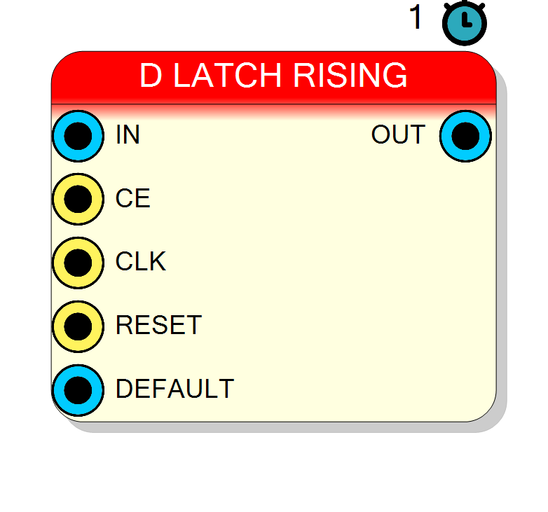
Level-sensitive transparent latch that stores multi-bit data values. When the clock enable signal is active, the output transparently follows the input. When disabled, the latch holds its current state. Supports configurable clock edge polarity and default reset values.
Introduction
This block implements a D-type latch for storing multi-bit data values. Unlike edge-triggered flip-flops, latches are level-sensitive storage elements that are transparent when enabled.
The latch operates as follows:
- When CE (clock enable) is HIGH (for rising edge) or LOW (for falling edge): Output = Input (transparent)
- When CE is inactive: Output holds its previous value (storage)
Key characteristics:
- Level-sensitive behavior (transparent latch)
- Configurable clock edge polarity (rising or falling)
- Synchronous reset with configurable default value
- Latency: 1 clock cycle
Pin Description
Clock Enable input (active high).
- CE = ‘1’: Latch is enabled (transparent mode)
- CE = ‘0’: Latch holds previous value Default: ‘1’ if left unconnected.
Properties
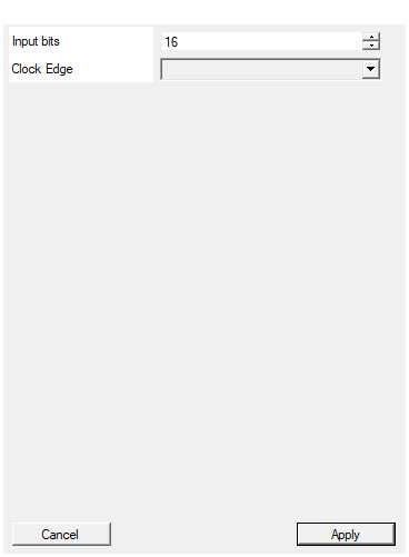
Set the number of bits of the input
Number of bits in the latch (width of IN, DEFAULT, and OUT). Range: 1-2048 bits.Default: 16
Range: 1 – 2048
Select between rising and falling edge
Clock edge polarity: RISING (latch operates on rising edges) or FALLING (latch operates on falling edges).Default: RISING
Options: RISING FALLING
Functional description
A D latch is a level-sensitive storage element, distinct from edge-triggered flip-flops. The component implements the following truth table:
Truth table (Rising Edge mode)
| CLK | CE | RESET | Behavior |
|---|---|---|---|
| X | X | 1 | OUT = DEFAULT |
| ↑ | 1 | 0 | OUT = IN (transparent) |
| ↑ | 0 | 0 | OUT = OUT(previous) |
Transparent operation
When the clock enable (CE) is active and the clock edge occurs:
- The latch is transparent: output tracks input continuously
- Changes on the input immediately propagate to the output
- This is fundamentally different from flip-flops which only capture on edges
Storage operation
When CE is inactive:
- The latch holds its current value
- Input changes are ignored
- The stored value is maintained until the next active clock cycle with CE asserted
Reset behavior
The component supports synchronous reset:
- When RESET = ‘1’, output is set to the DEFAULT value on the next active clock edge
- The DEFAULT value is configurable via the DEFAULT input pin
Clock edge polarity
The Edge property selects the clock polarity:
- RISING: Latch operates on rising clock edges (default)
- FALLING: Latch operates on falling clock edges
Timing
| Property | Latency (clock cycles) |
|---|---|
| D Latch | 1 |
The output updates one clock cycle after the input is sampled.
Latch vs Flip-Flop
Latches are level-sensitive:
- Transparent when enable is active (entire clock phase)
- Can lead to timing issues if not carefully controlled
- Used in specific design patterns (e.g., latch-based memories)
Flip-flops are edge-sensitive:
- Sample input only at clock edges
- Provide better timing isolation
- Preferred for most synchronous designs
Typical use cases
- Memory elements in latch-based register files
- Temporary storage in datapath logic
- Clock gating control (with careful timing analysis)
- Legacy designs requiring latch-based storage
- Interfacing with asynchronous logic (use with caution)
Design considerations
Warning: Latches can introduce timing hazards if not used carefully:
- Latch transparency can allow combinational glitches to propagate
- Hold time violations are more likely than with flip-flops
- Static timing analysis tools may flag latch-based designs
- Prefer flip-flops for synchronous digital designs unless latches are specifically required
Waveform example
Example with Input Size = 4 bits, Rising Edge mode, CE = ‘1’, showing transparent behavior:
The output follows the input after one clock cycle when CE is asserted.