
DSP - BLOCK LINEAR REGRESSION TM
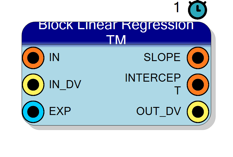
TM (time multiplexed) twin of Block Linear Regression: TM Factor (2..16) independent channels packed on one wide bus, each fitting the least-squares straight line x[i] = INTERCEPT + SLOPE*i against the sample index over its own block of N = 2^EXP samples (EXP on a runtime pin, shared by every lane). SLOPE is each lane’s drift rate in input units per sample; INTERCEPT is each lane’s fitted value at the first sample of the block - feed both to a downstream subtracter for per-lane drift removal. THERE IS NOT ONE MULTIPLIER IN THIS BLOCK, per lane or shared: the TM twin keeps the scalar’s two-cascaded-accumulator trick in every lane, and the only real arithmetic is the divisions, served by ONE shared restoring stage for all lanes. One shared frame - one EXP, one IN_DV, one OUT_DV per block - with per-lane accumulators at II=1 and ONE serial tail serving the lanes one after the other. Lane 0 sits in the LOW bits of every packed bus. Same per-lane numbers as the scalar twin, bit for bit. Optional shared BUSY / INTEGRATING / SAMPLE_COUNT status outputs.
Introduction
Per lane, over each block of N samples:
$$ x_i[k] \approx \mathrm{INTERCEPT}_i + \mathrm{SLOPE}_i \cdot k, \qquad k = 0 \dots N-1 \quad \text{(least squares, per lane)} $$
This is the time multiplexed (TM) twin of the scalar Block Linear Regression block: TM Factor independent channels packed on one wide bus, each fitting the least-squares line of its own block of N consecutive samples against the sample index. Nothing is shared between the channels except the frame.
As in the scalar twin - and in every lane - the regressor is the KNOWN sample index, so every sum over it is a closed form in N (a shift), and sum(i*x[i]) is reached with TWO CASCADED ACCUMULATORS per lane (R[k] = R[k-1] + x[k], A = sum of R[k]) instead of an index multiply. No multiplier anywhere; the two divisions by N(N^2-1) and N(N+1) are the only real arithmetic, and ONE shared restoring stage serves both quotients of every lane, reloaded between them.
The TM contract
INis TM Factor lanes of input width bits each, lane 0 in the LOW bits (lane 0 is the oldest sample of the clock) - the same packing as every other TM block in the toolchain. Each lane is an independent channel: its own R / A accumulator pair, its own fit.- ONE shared
EXPpin, ONEIN_DV, one frame: all lanes start and end their blocks on the same accepted clocks.BUSY,INTEGRATINGandSAMPLE_COUNTtherefore stay scalar -SAMPLE_COUNTcounts per-lane samples, which are identical in every lane by construction. Per lane, the index i counts ACCEPTED samples, not clocks: anIN_DVgap does not leave a hole in any lane’s regressor. - Accumulation runs at II=1 on the packed bus, one cascaded accumulator pair per lane. TM Factor times the accumulator registers is the unavoidable cost of TM state - and there is NO multiplier in the accumulation path of any lane.
- The serial post-processing is ONE shared engine serving the lanes one after the other: one restoring-division stage computes each enabled quotient of each lane in turn. It runs once per block, so lane-multiplexing it keeps the tail resources of the SCALAR block at the cost of tail latency x TM Factor.
- ONE
OUT_DVper block, after the LAST lane’s tail completes. All output lanes are staged as each lane finishes and committed together on theOUT_DVclock, so every packed output moves on that clock and no other.
N is a runtime input: the block size is $N = 2^{\mathrm{EXP}}$, EXP clamped to Max Block Exponent and latched on the first accepted sample of a block, so a change takes effect on the NEXT block - for every lane at once. The closed-form index sums are shifts because N is a power of two; the two division denominators genuinely are not, which is why the divider exists.
When to use this instead of TM Factor scalar blocks
One TM block and TM Factor scalar blocks compute the same numbers. The TM block pays the per-lane accumulators (unavoidable either way) but shares ONE frame, ONE control FSM and ONE serial divider across all lanes. The price is tail latency (TM Factor times the scalar tail) and the coupling of the frame: all lanes must share the same block length and the same sample cadence. Channels that need different block sizes need scalar blocks.
Pin Description
IN_DV is
high.
Properties
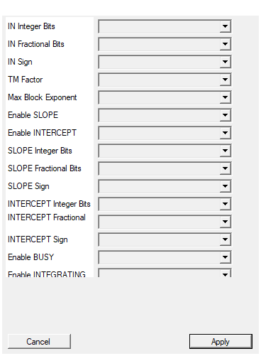
Number of INTEGER bits of the input sample (per lane) (the sign, when present, uses one of them).
Integer bits of ONE LANE of the input (the sign, when present, uses one of them). 1..64. Default 16.Default: 16
Options: 1 2 3 4 5 6 7 8 9 10 11 12 13 14 15 16 17 18 19 20 21 22 23 24 25 26 27 28 29 30 31 32 33 34 35 36 37 38 39 40 41 42 43 44 45 46 47 48 49 50 51 52 53 54 55 56 57 58 59 60 61 62 63 64
Number of FRACTIONAL bits of the input sample (per lane), i.e. the bits to the right of the binary point. Total width = integer + fractional bits, and must not exceed 64.
Fractional bits of one lane of the input. 0..64, total lane width 2..64 bits. Default 0.Default: 0
Options: 0 1 2 3 4 5 6 7 8 9 10 11 12 13 14 15 16 17 18 19 20 21 22 23 24 25 26 27 28 29 30 31 32 33 34 35 36 37 38 39 40 41 42 43 44 45 46 47 48 49 50 51 52 53 54 55 56 57 58 59 60 61 62 63 64
Select whether the input sample (per lane) is signed (two’s complement) or unsigned.
SIGNED (two’s complement) or UNSIGNED lanes. Default SIGNED. Applies to every lane.Default: SIGNED
Options: UNSIGNED SIGNED
Number of INDEPENDENT time-multiplexed channels packed on the IN bus and on every result bus. Lane 0 occupies the LOW bits (lane 0 = the oldest sample of the clock), the same packing as every other TM block. All lanes share one EXP / IN_DV / frame; each lane gets its own accumulators, but the serial post-processing is ONE engine serving the lanes one after the other, so the tail latency (and the minimum usable EXP) grows with this factor.
Number of independent channels packed on the buses, 2..16. Default 4. Multiplies the IN width, every packed output width AND the serial tail length (the shared divider serves the lanes one after the other), so it also raises the minimum usable EXP.Default: 4
Options: 2 3 4 5 6 7 8 9 10 11 12 13 14 15 16
Largest block-size exponent the accumulators are sized for: the block can be up to 2^MaxBlockExponent samples long. The EXP input is clamped to this value at run time. Raising it widens the internal accumulators, and ON THE BLOCKS WHOSE SERIAL ENGINES ARE SIZED FROM THOSE ACCUMULATORS (Coefficient of Variation, SNR, Skewness, Kurtosis, Correlation, Autocorrelation, Linear Regression) it also LENGTHENS THE SERIAL TAIL – even when the runtime EXP is small. Keep it at the largest block you actually use. The default of 20 covers blocks of up to 1048576 samples.
Largest block-size exponent the per-lane accumulators are sized for; the EXP input is clamped to it at run time. Raising it widens every lane’s cascaded accumulators AND lengthens the shared divider (CNUMW grows by two bits per unit). 1..31, default 20.Default: 20
Options: 1 2 3 4 5 6 7 8 9 10 11 12 13 14 15 16 17 18 19 20 21 22 23 24 25 26 27 28 29 30 31
YES: the the SLOPE output (per lane, packed) pin is present. NO: the pin AND all of its logic are removed BEFORE synthesis, so nothing is paid for it.
YES: the packed SLOPE bus exists. NO: its division, its pin and its clocks are removed - in every lane. Default YES.Default: YES
Options: NO YES
YES: the the INTERCEPT output (per lane, packed) pin is present. NO: the pin AND all of its logic are removed BEFORE synthesis, so nothing is paid for it.
YES: the packed INTERCEPT bus exists. NO: its division, its pin and its clocks are removed - in every lane. Default YES.Default: YES
Options: NO YES
Number of INTEGER bits of the SLOPE output (per lane) (the sign, when present, uses one of them).
Integer bits of ONE LANE of SLOPE. 1..64, default 8.Default: 8
Options: 1 2 3 4 5 6 7 8 9 10 11 12 13 14 15 16 17 18 19 20 21 22 23 24 25 26 27 28 29 30 31 32 33 34 35 36 37 38 39 40 41 42 43 44 45 46 47 48 49 50 51 52 53 54 55 56 57 58 59 60 61 62 63 64
Number of FRACTIONAL bits of the SLOPE output (per lane), i.e. the bits to the right of the binary point. Total width = integer + fractional bits, and must not exceed 64.
Fractional bits of one lane. 0..64, default 16 - a drift of less than one input LSB per sample is exactly what this block exists to measure, so the fractional bits are where the value lives. Each one also lengthens the shared divider by one clock per lane.Default: 16
Options: 0 1 2 3 4 5 6 7 8 9 10 11 12 13 14 15 16 17 18 19 20 21 22 23 24 25 26 27 28 29 30 31 32 33 34 35 36 37 38 39 40 41 42 43 44 45 46 47 48 49 50 51 52 53 54 55 56 57 58 59 60 61 62 63 64
Select whether the SLOPE output (per lane) is signed (two’s complement) or unsigned.
SIGNED or UNSIGNED lanes. Default SIGNED - a drift goes both ways.Default: SIGNED
Options: UNSIGNED SIGNED
Number of INTEGER bits of the INTERCEPT output (per lane) (the sign, when present, uses one of them).
Integer bits of ONE LANE of INTERCEPT. 1..64, default 16 (it lives in input units, so mirror the input range).Default: 16
Options: 1 2 3 4 5 6 7 8 9 10 11 12 13 14 15 16 17 18 19 20 21 22 23 24 25 26 27 28 29 30 31 32 33 34 35 36 37 38 39 40 41 42 43 44 45 46 47 48 49 50 51 52 53 54 55 56 57 58 59 60 61 62 63 64
Number of FRACTIONAL bits of the INTERCEPT output (per lane), i.e. the bits to the right of the binary point. Total width = integer + fractional bits, and must not exceed 64.
Fractional bits of one lane. 0..64, default 8. Each one also lengthens the shared divider by one clock per lane.Default: 8
Options: 0 1 2 3 4 5 6 7 8 9 10 11 12 13 14 15 16 17 18 19 20 21 22 23 24 25 26 27 28 29 30 31 32 33 34 35 36 37 38 39 40 41 42 43 44 45 46 47 48 49 50 51 52 53 54 55 56 57 58 59 60 61 62 63 64
Select whether the INTERCEPT output (per lane) is signed (two’s complement) or unsigned.
SIGNED or UNSIGNED lanes. Default SIGNED.Default: SIGNED
Options: UNSIGNED SIGNED
YES: the BUSY (high from the first sample of a block until its result is out – it COVERS THE SERIAL TAIL, and its last high clock IS the OUT_DV pulse) pin is present. NO: the pin AND all of its logic are removed BEFORE synthesis, so nothing is paid for it.
YES: the shared BUSY pin exists. Default NO.Default: NO
Options: NO YES
YES: the INTEGRATING (high only while the block is ACCUMULATING; it drops as soon as the N-th sample has been taken and the tail starts, so BUSY-and-not-INTEGRATING means ‘computing’) pin is present. NO: the pin AND all of its logic are removed BEFORE synthesis, so nothing is paid for it.
YES: the shared INTEGRATING pin exists. Default NO.Default: NO
Options: NO YES
YES: the SAMPLE_COUNT (32 bit, how many samples have been accumulated so far in the current block: 1 after the first, N after the N-th. It is NOT cleared at the block end – it holds N until the NEXT block’s first accepted sample takes it back to 1. On a CONTINUOUS stream that happens DURING the serial tail, so at OUT_DV it reads how far into the next block the input has already got, NOT N. To capture the length of the block being presented, latch SAMPLE_COUNT on the clock INTEGRATING falls – that one always reads N) pin is present. NO: the pin AND all of its logic are removed BEFORE synthesis, so nothing is paid for it.
YES: the shared 32 bit SAMPLE_COUNT pin exists. Default NO.Default: NO
Options: NO YES
ROUND: round to nearest when a result has to be requantised into a coarser output format. TRUNCATE: drop the bits (cheaper, adds a negative bias).
ROUND: round to nearest at each lane’s final requantisation - real on this block, because both divisions carry guard bits underneath the requested format. TRUNCATE: drop the bits. Default ROUND.Default: ROUND
Options: TRUNCATE ROUND
YES: clip to the largest representable value of each output format (symmetric for signed formats). NO: wrap around.
YES: clip each lane to its output format (symmetric for signed). NO: wrap. Default YES.Default: YES
Options: NO YES
Accuracy, per lane
Each lane carries the scalar twin’s bound: everything before the divisions is exact integer arithmetic (cascaded accumulators, closed-form denominators, Sw - shifts and adds only), both divisions carry SQG = 4 guard bits underneath the requested Q format, and the result is requantised with the selected rounding - so each lane’s SLOPE and INTERCEPT are within 1 LSB of the exactly-rounded values. Each lane is bit-identical to the scalar twin run on the same lane stream. (Unlike the ratio blocks of this family, the Rounding property is REAL here - the guard bits leave something to round.)
Timing: the TM latency contract
OUT_DV pulses ONCE per block, L clocks after the clock on which the
N-th sample was accepted, where
$$ L = 1 + \mathrm{TM},\bigl(2 + (\mathrm{EN_{SLOPE}} + \mathrm{EN_{INTERCEPT}})\cdot\mathrm{CNUMW}\bigr) $$
(BLRT_TAIL in the core). Per lane: CALC, then one CNUMW-clock restoring
division per ENABLED output out of the ONE shared stage, then FIN - the
family’s lane-multiplexed rule
$L_{tm}(e) = \mathrm{TM},(L_{scalar}(e)-1)+1$. The step count is COMPILE
TIME: it does NOT depend on the runtime exponent. At the defaults (16 bit
signed input, Q8.16 SLOPE, Q16.8 INTERCEPT, Max Block Exponent 20, TM 4,
both outputs on) CNUMW = 81, so L = 1 + 4164 = 657 clocks, minimum usable
EXP 10; turn one output off and L = 1 + 483 = 333, minimum EXP 9.
Disabling an output removes its division, its pin and its clocks - in
every lane at once.
The family drop rule applies with the TM tail: the tail of one block must
finish before the NEXT block completes, $2^{{\mathrm{{EXP}}}} \ge L$, or the
completing block’s result is silently DROPPED (no OUT_DV, accumulators
unaffected, no error pin). The TM tail makes the minimum usable EXP larger
than the scalar twin’s - the compiler prints both the worst-case tail and
the minimum EXP in the compilation log, and the property window refuses a
configuration whose minimum exceeds Max Block Exponent.
Knowing where the block is: BUSY, INTEGRATING and SAMPLE_COUNT
Identical to the scalar family, and SHARED by all lanes: INTEGRATING is
high exactly while the block is accumulating (it dips one clock per block
boundary on a continuous stream), BUSY also covers the (TM-long) tail and
its last high clock IS the OUT_DV pulse, SAMPLE_COUNT reads 1 after the
first accepted sample and N after the N-th.
SAMPLE_COUNTis NOT cleared at the block end - it holds N until the NEXT block’s first accepted sample takes it back to 1. On a CONTINUOUS stream that happens DURING the serial tail (which on a TM block is TM Factor times longer), so atOUT_DVit reads how far into the next block the input has got, NOT N. The clock that always reads N is the oneINTEGRATINGfalls on - latch it there.
Verification
The core is regression tested by a host-side csim harness
(tb/block-ops-tm/run_tb_tm.ps1) with per-lane goldens computed by
gen_golden_tm.py in exact rational arithmetic ON EACH LANE’S STREAM ALONE
(lanes deliberately carry different signals - the generator refuses
identical lanes), solved from the NORMAL EQUATIONS, never from the
cascaded-accumulator identity the core uses - so the algebra is checked
against an independent derivation. Plus the strongest available
lane-independence check: after every run, the SCALAR twin is replayed on
each lane’s stream by itself and lane k of every TM result must match it
BIT FOR BIT. The status waveform is checked clock by clock, every packed
output is checked to move only on OUT_DV, and the TM-specific mutant
classes (shared accumulator, lane swaps, wrong-lane tail reads, early
commit, drop rule) are killed. What no host harness can prove - that Vitis
accepts and schedules the core at II=1 - is stated in AGENT/block_ops.log,
not silently implied.