
Fixed to Float TM
Time-multiplexed fixed-point to floating-point converter based on Xilinx Floating Point IP. Supports single (32-bit) and double (64-bit) precision, configurable input bit width, and multiple TM phases (1-32) for high-throughput parallel conversion in digital signal processing pipelines.
Introduction
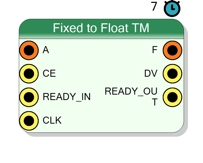
This block converts fixed-point integer values to IEEE 754 floating-point representation using the Xilinx Floating Point IP core. The component supports Time Multiplexing (TM): multiple parallel conversion units (phases) share the same clock cycle, enabling high sample rates with predictable latency.
On every rising edge of CLK, if CE = 1 and READY_IN = 1, the converter
performs
$$ \mathrm{F}(n) = \text{float}\bigl(\mathrm{A}(n)\bigr), $$
where $\mathrm{A}$ is the fixed-point input (treated as integer with 0 fractional bits) and $\mathrm{F}$ is the IEEE 754 output. The TM Factor property determines how many parallel instances are instantiated.
Pin Description
Fixed-point input data.
- If Input is TM = true: TM bus of width
BitWidth × TMFactor - If Input is TM = false: Scalar of width
BitWidth(replicated to all phases) Interpreted as signed or unsigned integer with 0 fractional bits.
CE = 0 the converter pipeline is stalled.
Maps to s_axis_a_tvalid in the AXI Stream interface.
m_axis_result_tready. Default: ‘1’ if not connected.
Floating-point output (IEEE 754), always TM.
Width: (Exponent + Mantissa) × TMFactor
- Single: 32 bits/phase → total 32×TMFactor
- Double: 64 bits/phase → total 64×TMFactor Valid after 7 clock cycles from input.
m_axis_result_tvalid signals.
s_axis_a_tready signals.
Properties
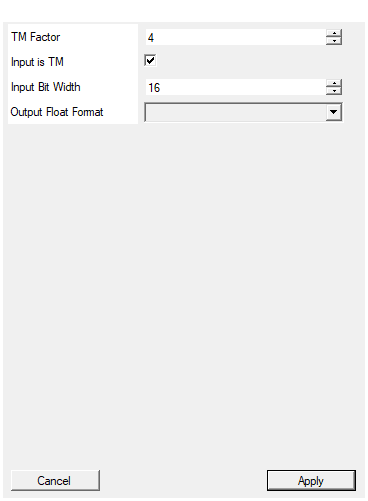
Time Multiplexing factor of the input (number of phases)
Number of time-multiplexed phases (parallel conversion units). Range: 1 – 32. Higher values increase throughput proportionally but consume more FPGA resources (N instances of the Xilinx IP).Default: 4
Range: 1 – 32
If true, input is Time Multiplexed. If false, input is a simple non-TM float
Selects input mode:
true→ InputAis a TM bus; each phase gets its slicefalse→ InputAis scalar; replicated to all phases
Default: True
Bit width of the input (for TM, this is the width of each phase)
Bit width of each fixed-point input sample ($N_\text{in}$). Range: 1 – 128. This sets the Input Exponent Width in the Xilinx IP (with Fraction Width = 0).Default: 16
Range: 1 – 128
Select between single precision 32 bit and double precision 64 bit
Output floating-point format:
Single→ IEEE 754 single precision (32-bit): 8 exp + 24 mantissaDouble→ IEEE 754 double precision (64-bit): 11 exp + 53 mantissa
Internally mapped to Result_Precision_Type, C_Result_Exponent_Width,
and C_Result_Fraction_Width in the Xilinx Floating Point IP configuration.
Default: Single
Options: Single Double
Functional description
The component wraps the Xilinx Floating Point IP (operation type: Fixed_to_float)
and replicates it N times (where N = TM Factor) to support time-multiplexed
data streams.
Input modes
- Input is TM = true: The input
Ais a TM bus of widthBitWidth × TMFactor. Each phase receives its corresponding slice. - Input is TM = false: The input
Ais a scalar signal of widthBitWidth, replicated to all TM phases for parallel conversion.
Output
The output F is always TM, with width (Exponent + Mantissa) × TMFactor:
- Single precision: 32 bits per phase (8 exp + 24 mantissa)
- Double precision: 64 bits per phase (11 exp + 53 mantissa)
Data valid and ready handshake
CE(input): Clock enable, controls all phases togetherDV(output): Data valid, asserted when all phases have valid outputREADY_OUT(output): Ready to accept new input (AND of all phase ready signals)READY_IN(input): Downstream ready signal
Mathematical background
For a fixed-point input $x$ interpreted as an integer, the conversion produces:
$$ f = x \times 2^0 = x, $$
stored in IEEE 754 format:
- Single: 1 sign bit + 8 exponent bits + 23 fraction bits (24-bit mantissa including implicit 1)
- Double: 1 sign bit + 11 exponent bits + 52 fraction bits (53-bit mantissa including implicit 1)
The fixed input is assumed to have Exponent Width = BitWidth and Fraction Width = 0
in the Xilinx IP configuration.
Timing
The Xilinx Floating Point IP has a fixed latency of 7 clock cycles per phase:
| Property | Latency (clock cycles) |
|---|---|
| Fixed to Float | 7 |
Total system delay: T_delay = 7 × T_CLK.
In TM mode, all phases operate in parallel with the same latency, producing
TMFactor outputs per cycle after the initial pipeline fill.
Typical use cases
- High-speed ADC data conversion to floating-point for DSP algorithms
- Nuclear/particle physics detectors with multi-channel readout
- Signal processing front-ends requiring floating-point arithmetic
- Scientific instrumentation with time-multiplexed data acquisition
Waveform example
Example with TM Factor = 4, Input is TM = true, BitWidth = 16, Single precision.
Note: 7 clock cycles of latency from input to output.