
ROM (Read-Only Memory)
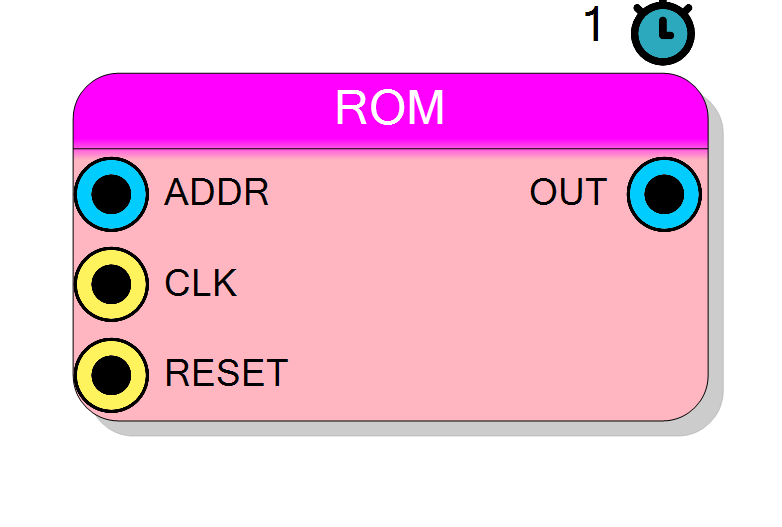
Read-only memory initialized from user-provided data file. Stores constant data that cannot be modified at runtime. Data is read using the ADDR input with 1 clock cycle latency. Content is loaded from a text file (decimal or hexadecimal format) during FPGA compilation.
Introduction
This block implements non-volatile read-only memory initialized with user data during FPGA compilation. The ROM contents are fixed and cannot be modified at runtime.
Read latency: 1 clock cycle.
Pin Description
Properties
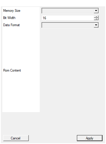
Set the amount of memory in number of words
Number of words in ROM. Allowed: 4-65536. Must match data file size.Default: 1024
Options: 4 8 16 32 64 128 256 512 1024 2048 4096 8192 16384 32756 65536
Set the size in bits of the data
Bit width per word. Range: 1-1024 (maximum 256 in legacy docs).Default: 16
Range: 1 – 1024
Select data format as Decimal or Hexadecimal
Data format: HEX, SIGNED DECIMAL, or DECIMAL. Must match format used in RomContent file.Default: HEX
Options: HEX SIGNED DECIMAL DECIMAL
Functional description
ROM stores constant data loaded from a text file:
- Each line in the file = one memory word
- Supports decimal or hexadecimal format
- Data is synthesized into FPGA block RAM
- Read-only: No write capability
Data file format
Create a .txt file with one value per line:
A012
0012
0133
F0F1
(Example in hexadecimal format, no “0x” prefix)
Timing
Read: Apply address on ADDR; data appears on OUT 1 cycle later.
Typical use cases
- Lookup tables (LUTs)
- Coefficient storage for filters
- Calibration constants
- Waveform tables