
LFSR / PRBS
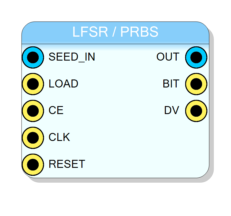
Classic single maximal-length LFSR with configurable register length (3..64): one step per CE clock, period 2^Length - 1, whole-register PRBS word plus the serial PRBS bit on separate pins. Initial seed from a property (auto-randomized at placement); a new seed can be loaded at any time at runtime through the SEED_IN bus and the LOAD pin. Pure VHDL, a handful of flip-flops and XORs.
Introduction
A linear feedback shift register with the XAPP052 maximal-length tap set:
for every Length $n$ from 3 to 64 the sequence walks through all
$2^n - 1$ nonzero states before repeating. Every CE clock advances the
register by one step (DV marks it):
OUTis the whole register — a PRBS word, handy as a cheap wide stimulus or address/pattern scrambler;BITis the freshly generated feedback bit — the classic serial PRBS-n bit stream (PRBS7, PRBS15, PRBS23, PRBS31 … depending on Length) used for bit-error-rate testing and link bring-up.
Being a single linear recurrence, an LFSR is spectrally flat but has a strong algebraic structure (each output bit is the same sequence delayed). When statistical quality matters, use the Uniform Random block; use this one when you want the standard PRBS sequences, the smallest possible footprint, or an exactly known period.
Seeding
- The SEED property sets the state loaded by
RESET. It is randomized automatically when the block is placed and is forced nonzero (the all-zero state would lock a XOR-feedback LFSR). - At runtime, drive
SEED_INwith a new value and pulseLOADfor one clock: the register reloads instantly and the sequence continues from the new seed (LOADwins overCE;DVis suppressed on the load cycle). An all-zeroSEED_INis silently replaced with 1, so the generator can never lock up. Connect the bus to a register block to re-seed from software.
The tap table is validated offline (exhaustive period check up to n = 20, algebraic maximality check for every length up to 64) and the hardware is verified against an independent Python reference: golden vectors, runtime-load semantics, zero-seed sanitization and the measured full period (255 at n = 8, 65535 at n = 16) in a self-checking GHDL regression, mutation-tested.
Pin Description
Properties
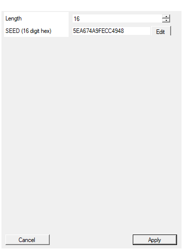
LFSR register length (3..64). Maximal-length taps: the sequence repeats after 2^Length - 1 steps. Sets the width of OUT and SEED_IN.
Register length n (3..64). Maximal taps (XAPP052): period is exactly 2^n - 1. Sets the width of OUT and SEED_IN.Default: 16
Range: 3 – 64
Initial LFSR state (64-bit hex, truncated to Length bits, forced nonzero). Automatically randomized when the component is created. RESET restarts from this seed; a different seed can be loaded at runtime through SEED_IN + LOAD.
Initial state as a hex number (up to 16 digits, truncated to Length bits, forced nonzero). Auto-randomized when the component is created; editable for reproducible sequences.Default: 5EA674A9FECC4948
Usage notes
- Leaving
CEunconnected ties it to ‘1’ (one step per clock);LOADdefaults to ‘0’. - The serial stream on
BITequals the LSB ofOUTon every DV cycle. - Two instances with different seeds produce the SAME sequence at different phases (that is the nature of an LFSR): for independent streams use two different Lengths, or the Uniform Random block.
RESETmakes runs reproducible: the sequence always restarts from the SEED property.