
A395B - LVDS Output Expansion
32-channel LVDS output expansion board for V2495. Drives external equipment with differential LVDS signals from the FPGA logic.
Introduction
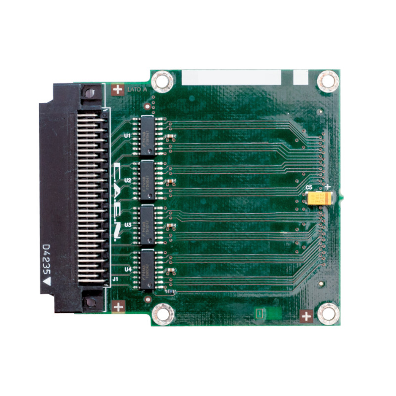
The A395B is an expansion board for the V2495 that provides 32 LVDS output channels. It can be installed in expansion slots D, E, or F of the V2495 mainboard.
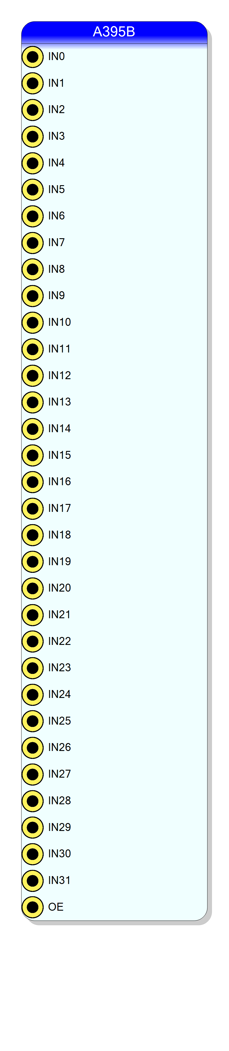
From the FPGA perspective, this board drives external signals. The 32 channels appear as inputs to the block (receiving data from your logic design) plus an Output Enable (OE) control.
Product link: CAEN A395B
Pin Description
Output Enable control.
- HIGH (1): The P/N terminals drive the INx values
- LOW (0): The P/N terminals are in three-state (high-Z)
Use this to control when the outputs are active.
Input signals from FPGA logic (32 total). Each channel is a 1-bit signal to be driven to the external output.
Connect your logic outputs to drive the LVDS differential pairs.
Properties
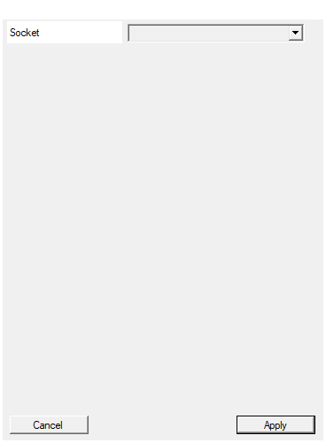
Select the socket hosting the expansion board
Selects the expansion socket where the A395B is installed. Available options: D, E, F. Must match the physical installation location on the V2495 mainboard.Default: D
Options: D E F
Usage
Signal Direction
The A395B is an output expansion - it drives signals to external equipment via LVDS differential pairs. From the SciCompiler perspective:
┌──────────────────────────────────────────────────────────────────┐
│ A395B Signal Flow │
│ │
│ ┌─────────────┐ ┌─────────────┐ External │
│ │ FPGA │ │ │ Equipment │
│ │ Logic │═══► IN0-IN31 ═══►│ A395B │═══► │
│ │ │ │ (32 ch) │ LVDS │
│ │ │═══► OE ─────────►│ │ Signals │
│ └─────────────┘ └─────────────┘ │
└──────────────────────────────────────────────────────────────────┘
Output Enable (OE)
The OE (Output Enable) pin controls the output driver state:
| OE State | Behavior |
|---|---|
| HIGH (1) | Outputs are driven with INx values |
| LOW (0) | Outputs are in three-state (high impedance) |
Expansion Socket Selection
The A395B can be installed in one of three expansion sockets:
| Socket | Description |
|---|---|
| D | Expansion slot D |
| E | Expansion slot E |
| F | Expansion slot F |
Select the appropriate socket during block creation to match the physical installation.
Signal Characteristics
| Parameter | Value |
|---|---|
| Channels | 32 |
| Signal type | LVDS (differential) |
| Direction | Output from V2495 |
| Output control | Three-state via OE |
Typical Usage
Connect FPGA logic outputs to drive external equipment via LVDS:
FPGA trigger/pulse logic ──► A395B ──► External NIM/VME modules
Resources & Timing
-
Latency: Minimal (output buffer delay only)
-
Throughput: 32 channels at FPGA clock rate
- LVDS differential output standard
- Three-state control via OE pin
- Each channel independently driven from FPGA
Supported Boards
- V2495