
List DMA
High-performance FIFO-based data transfer block using DMA channels for maximum throughput. Uses one of 4 available DMA channels per DAQ board. Only available on DT5560/R5560 boards.
Introduction
Principle of Operation
The List DMA block is a high-performance variant of the standard List block that uses Direct Memory Access (DMA) channels for data transfer. This enables significantly higher throughput compared to register-based transfers.
DMA Channel Selection
Each DT5560/R5560 DAQ board provides 4 DMA channels (0-3). When using this block, you must select which DMA channel to use in the properties. Each DMA channel can only be used by one endpoint in the entire design.
Important Constraints:
- Maximum 4 List DMA blocks per DAQ board
- Each block must use a different DMA channel
- DMA channels are shared resources - plan your design accordingly
List DMA vs Standard List
| Feature | List DMA | Standard List |
|---|---|---|
| Transfer method | DMA (64-bit) | Register FIFO |
| Throughput | Higher | Standard |
| DMA channel required | Yes (1 of 4) | No |
| Maximum per board | 4 | Unlimited |
| Board compatibility | DT5560/R5560 only | All boards |
| Best for | High-rate streaming | General purpose |
The List DMA data can be read via Resource Explorer or programmatically using the SciSDK library.
SciSDK Documentation: https://nuclearinstruments.github.io/SCISDK/
Pin Description
Data Input – Input data word to be written to the FIFO. Size is configurable (32 to 256 bits).
Data is captured on the clock edge when WR is HIGH.
Write Enable – When HIGH (and acquisition is enabled), the value on IN is written to the FIFO on the clock edge.
If FIFO is full, data is lost.
Busy – HIGH when the block is not accepting data.
This signal is HIGH when:
- Acquisition is disabled (
CONFIG[0] = 0), OR - FIFO is full
Logic: BUSY = NOT CONFIG[0] OR FULL
Use this signal to gate your data source when the List cannot accept more data.
Properties
Select the DMA channel to use for data transfer (0-3).
Important: Each DMA channel can only be used by one endpoint in the entire design. Make sure to assign different channels to each List DMA block.
Available values: 0, 1, 2, 3 Default: 0
FIFO buffer depth in words. Available values: 128, 256, 512, 1024, 2048, 4096, 8192, 16384, 32768, 65536.
Larger buffers compensate for readout bus stalls but use more FPGA resources. Default: 1024
Input data word size in bits. Available values: 32, 64, 96, 128, 160, 192, 224, 256.
Larger words are converted to multiple 64-bit DMA transfers internally. Default: 32
⚙️ Detailed Operation
Data Flow
┌──────────────────────────────────────────────────────────────────┐
│ List DMA Data Flow │
│ │
│ IN (32-256 bits) ───►┌──────────┐ ┌─────────────┐ │
│ │ │ │ │ │
│ WR ─────────────────►│ FIFO │────►│ DMA Engine │───► PC │
│ │ Buffer │ │ (64-bit) │ │
│ CLK ────────────────►│ │ │ │ │
│ RESET ──────────────►└──────────┘ └─────────────┘ │
│ │ │
│ ┌────┴────┐ │
│ │ FULL │──► HIGH when buffer full │
│ │ BUSY │──► HIGH when not accepting │
│ └─────────┘ │
└──────────────────────────────────────────────────────────────────┘
Write Operation
- Acquisition must be started via software (CONFIG register bit 0 = 1)
- When WR goes HIGH, the value on IN is written to the FIFO
- Data is transferred to PC via DMA as 64-bit words
- FULL goes HIGH if the FIFO overflows (data loss!)
Signal Timing
The internal write signal is generated by the following logic:
iWRITE = CONFIG[0] AND WR AND (NOT FULL)
This means data is written to the FIFO only when all three conditions are true:
- Acquisition is enabled (
CONFIG[0] = 1) - Write request is active (
WR = 1) - FIFO is not full (
FULL = 0)
Output signals logic:
| Signal | Logic | Description |
|---|---|---|
BUSY |
NOT CONFIG[0] OR FULL |
HIGH when stopped OR full |
FULL |
Internal FIFO full flag | HIGH when buffer overflows |
Important: The BUSY signal is HIGH when acquisition is disabled (stopped state),
which indicates that the block is not accepting new data. It also goes HIGH when the FIFO is full.
Timing Diagrams
Normal Write Sequence:
FIFO Full Condition:
Word Size and DMA Conversion
The input word size is configurable from 32 to 256 bits. Internally, words are converted to 64-bit DMA transfers:
| Input Size | 64-bit DMA Words per Sample |
|---|---|
| 32 bits | 0.5 (packed) |
| 64 bits | 1 |
| 128 bits | 2 |
| 256 bits | 4 |
Important: The DMA engine transfers data in 64-bit words, providing higher bandwidth than the 32-bit register interface of the standard List block.
Configuration Registers
CONFIG
| Bit | Function |
|---|---|
| 0 | Enable acquisition (1 = running, 0 = stopped) |
| 1 | Force reset |
STATUS
| Bit | Function |
|---|---|
| 0 | Empty (1 = FIFO empty) |
| 1 | Full (1 = FIFO full) |
| 31:8 | Available words count |
Software Integration with SciSDK
The List DMA is fully supported by SciSDK. The API is identical to the standard List. For complete documentation see: SciSDK List Guide
Available Parameters
| Parameter | Access | Description | Default |
|---|---|---|---|
acq_len |
R/W | Maximum samples per FIFO read | 1024 |
acq_mode |
R/W | blocking or non-blocking |
blocking |
timeout |
R/W | Timeout in ms for blocking mode | 100 |
thread |
R/W | Enable internal threading for high performance | false |
high_performance |
R/W | Priority bus access mode | false |
threaded_buffer_size |
R/W | Internal buffer size in dwords | 100000 |
Available Commands
| Command | Description |
|---|---|
start |
Clear FIFO and begin acquisition |
stop |
Stop acquisition |
C/C++ Example
c
#include "SciSDK_DLL.h"
// Define data structure matching FPGA word
#pragma pack(push, 1)
typedef struct {
uint32_t timestamp;
uint16_t energy;
uint16_t channel;
} EVENT_DATA; // 64 bits
#pragma pack(pop)
// Allocate buffer (1024 samples)
SCISDK_LIST_RAW_BUFFER *buffer;
SCISDK_AllocateBufferSize("board0:/MMCComponents/List_0",
T_BUFFER_TYPE_RAW,
(void**)&buffer, _sdk, 1024);
// Configure
SCISDK_SetParameterString("board0:/MMCComponents/List_0.acq_mode",
"blocking", _sdk);
SCISDK_SetParameterInteger("board0:/MMCComponents/List_0.timeout",
1000, _sdk);
// Start acquisition
SCISDK_ExecuteCommand("board0:/MMCComponents/List_0.start", "", _sdk);
// Read data
while (running) {
int ret = SCISDK_ReadData("board0:/MMCComponents/List_0",
(void*)buffer, _sdk);
if (ret == NI_OK && buffer->info.valid_samples > 0) {
// Cast raw data to our structure
EVENT_DATA *events = (EVENT_DATA*)buffer->data;
for (int i = 0; i < buffer->info.valid_samples; i++) {
printf("Event %d: ch=%d, energy=%d, ts=%u\n",
i, events[i].channel, events[i].energy,
events[i].timestamp);
}
}
}
// Stop and free
SCISDK_ExecuteCommand("board0:/MMCComponents/List_0.stop", "", _sdk);
SCISDK_FreeBuffer("board0:/MMCComponents/List_0",
T_BUFFER_TYPE_RAW, (void**)&buffer, _sdk);
Python Example
python
from scisdk.scisdk import SciSDK
import struct
sdk = SciSDK()
sdk.AddNewDevice("usb:10500", "dt5560", "board0", "RegisterFile.json")
# Allocate buffer
res, buf = sdk.AllocateBufferSize("board0:/MMCComponents/List_0",
sdk.T_BUFFER_TYPE_RAW, 1024)
# Configure
sdk.SetParameter("board0:/MMCComponents/List_0.acq_mode", "blocking")
sdk.SetParameter("board0:/MMCComponents/List_0.timeout", 1000)
# Start and read
sdk.ExecuteCommand("board0:/MMCComponents/List_0.start", "")
res, buf = sdk.ReadData("board0:/MMCComponents/List_0", buf)
if res == 0 and buf.info.valid_samples > 0:
# Interpret raw data (example: 64-bit words)
word_size = 8 # bytes per word
for i in range(buf.info.valid_samples):
offset = i * word_size
# Unpack as little-endian: timestamp(32), energy(16), channel(16)
ts, energy, ch = struct.unpack('<IHH', buf.data[offset:offset+word_size])
print(f"Event {i}: ch={ch}, energy={energy}, timestamp={ts}")
sdk.ExecuteCommand("board0:/MMCComponents/List_0.stop", "")
Resource Explorer
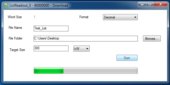
The List Module tool in Resource Explorer provides real-time data visualization and can save data to file.
Quick Reference
| Item | Description |
|---|---|
| Transfer method | DMA (64-bit words) |
| Word size | 32, 64, 128, 256 bits |
| DMA channels | 4 per board (0-3) |
| Data format | User-defined (raw bytes) |
| Best for | High-rate streaming |
Resources & Timing
-
Latency: 1 clock cycle write latency
-
Throughput: Higher than standard List due to DMA transfers
- Only available on DT5560/R5560 boards
- Uses one of 4 DMA channels per board
- Each DMA channel can only be used by one endpoint
- Maximum 4 List DMA blocks per DAQ board
- 64-bit DMA transfers for higher bandwidth
- Uses BRAM for FIFO storage
- Monitor FULL signal to prevent data loss