
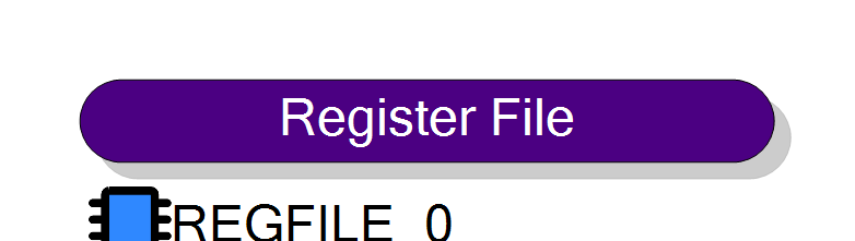
Register File
Creates multiple heterogeneous registers with a single schematic block. Each register can have different names, sizes, directions, and data types.
Introduction
The Register File block allows you to create multiple heterogeneous registers with a single component in the schematic. Instead of placing individual register blocks for each configuration parameter, you can define all registers in one place with a convenient graphical editor.
This is ideal when you need to manage many different configuration parameters, each with its own:
- Name (e.g., THRESHOLD, GAIN, ENABLE, MODE)
- Size (1 to 32 bits)
- Direction (input to FPGA or output from FPGA)
- Data type (bit vector or integer)
Pin Description
Dynamic pins created based on register definitions.
- OUT registers: Output pins carrying configuration values
- IN registers: Input pins for status/readback values Pin names match the register names defined in the editor.
Properties
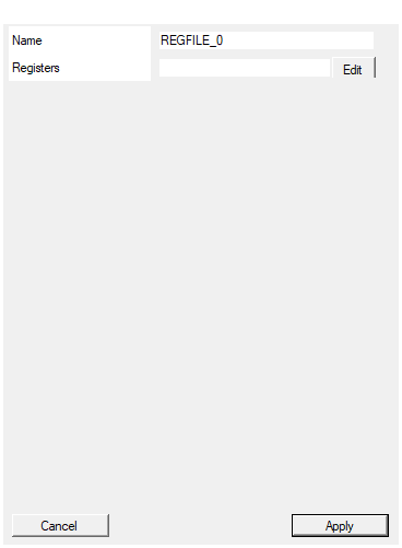
Set the name of the endpoint
Default: REGFILE_0
Define registers name and size
"ADC_CONFIG" generates SCI_REG_ADC_CONFIG_xxx.
Default: REGFILE_0.
Opens the Register Editor dialog to define the registers. Each register has:
- Name: Unique identifier (used in SDK)
- Direction: IN (input to block) or OUT (output from block)
- Type: BIT VECTOR or INTEGER
- Size: Bit width (1-32 for bit vector)
Usage
When to Use Register File
Use the Register File when you need to:
- Group related parameters: Keep all configuration registers for a subsystem together
- Manage diverse registers: Different sizes, types, and directions in one block
- Simplify schematics: Reduce visual clutter from multiple individual register blocks
- Organize memory map: All registers share a common base address with sequential offsets
Register File vs Single Registers
| Approach | Use Case |
|---|---|
| Register File | Many heterogeneous parameters (different names, sizes, types) |
| Single Register | One or few parameters with unique characteristics |
| CH-Register | Many channels of the same parameter (e.g., 16 thresholds) |
The Register Editor
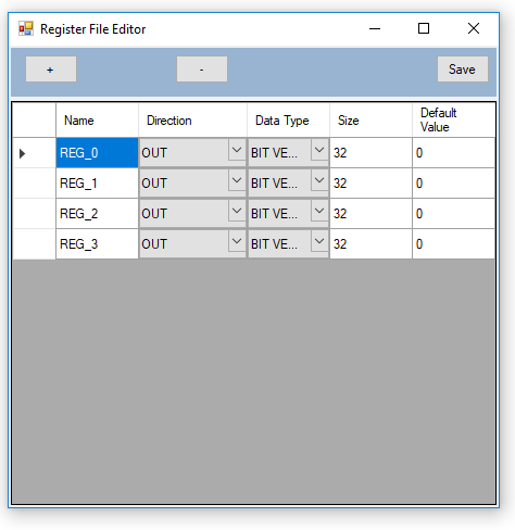
Click on the Registers property to open the configuration dialog:
The editor allows you to:
| Action | Description |
|---|---|
| Add Register | Create a new register entry |
| Remove Register | Delete selected register |
| Edit Name | Set meaningful parameter name |
| Select Direction | IN (read from FPGA) or OUT (write to FPGA) |
| Set Type | BIT VECTOR or INTEGER |
| Set Size | Bit width (1-32 for bit vector, ignored for integer) |
Direction Explained
| Direction | Symbol Pin | Software Access | Use Case |
|---|---|---|---|
| OUT | Output from block | Read/Write from software | Configuration parameters, thresholds, enables |
| IN | Input to block | Read-only from software | Status, counters, readback values |
OUT registers: Software writes a value → appears on the output pin IN registers: FPGA signal connected to input pin → software reads the value
Memory Mapping
All registers in a Register File share a common base address with sequential offsets:
Base Address: 0x1000 (assigned by compiler)
Register Layout:
┌─────────────────┬──────────┬────────┐
│ Register Name │ Offset │ Address│
├─────────────────┼──────────┼────────┤
│ THRESHOLD │ +0 │ 0x1000 │
│ GAIN │ +1 │ 0x1001 │
│ ENABLE │ +2 │ 0x1002 │
│ MODE │ +3 │ 0x1003 │
│ STATUS │ +4 │ 0x1004 │
└─────────────────┴──────────┴────────┘
This makes it easy to:
- Find related registers in the memory map
- Loop through registers programmatically
- Document the configuration interface
Practical Example: ADC Channel Configuration
Scenario: Configure a multi-channel ADC with various parameters
Register File: "ADC_CONFIG"
┌─────────────────┬───────────┬──────────┬──────┐
│ Name │ Direction │ Type │ Size │
├─────────────────┼───────────┼──────────┼──────┤
│ SAMPLE_RATE │ OUT │ INTEGER │ - │
│ TRIGGER_LEVEL │ OUT │ BIT VEC │ 16 │
│ TRIGGER_MODE │ OUT │ BIT VEC │ 2 │
│ CHANNEL_ENABLE │ OUT │ BIT VEC │ 8 │
│ PRETRIGGER │ OUT │ INTEGER │ - │
│ POSTTRIGGER │ OUT │ INTEGER │ - │
│ ARMED │ IN │ BIT VEC │ 1 │
│ TRIGGER_COUNT │ IN │ INTEGER │ - │
└─────────────────┴───────────┴──────────┴──────┘
Resulting schematic block:
┌─────────────────────────┐
│ Register File │
│ "ADC_CONFIG" │
├─────────────────────────┤
│ ARMED ─────► │ (IN: status)
│ TRIGGER_COUNT ─► │ (IN: counter)
│ │
│ ◄── SAMPLE_RATE │ (OUT: config)
│ ◄── TRIGGER_LEVEL │ (OUT: config)
│ ◄── TRIGGER_MODE │ (OUT: config)
│ ◄── CHANNEL_ENABLE │ (OUT: config)
│ ◄── PRETRIGGER │ (OUT: config)
│ ◄── POSTTRIGGER │ (OUT: config)
└─────────────────────────┘
Resources & Timing
-
Latency: 1 clock cycle (synchronous to bus clock)
-
Throughput: 1 register access per bus cycle
No FPGA fabric resources - registers are mapped directly to the bus interface. Compile generates SDK address definitions automatically.