
TDC Synchronous
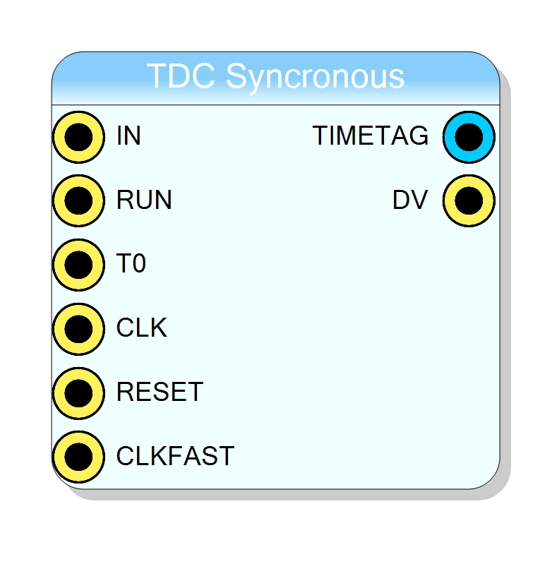
TDCSync is a Time-to-Digital Converter that timestamps digital input signals using a high-frequency counter. A 48-bit timestamp is captured on each input edge transition. The block supports multiple clock source options and includes built-in clock domain crossing (CDC) logic for reliable data transfer.
Introduction
TDCSync implements a synchronous Time-to-Digital Converter suitable for timestamping digital pulses with high resolution.
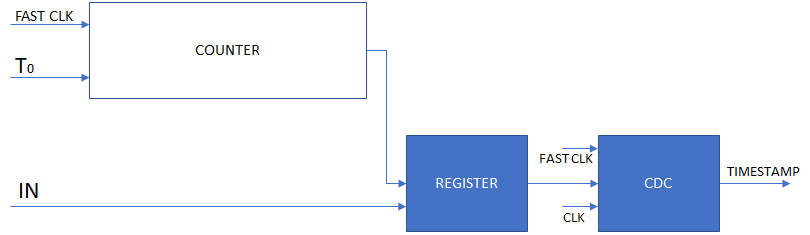
The core functionality is based on a 48-bit free-running counter clocked by a fast clock source. When an input signal transition is detected, the current counter value is latched and transferred to the output domain through a CDC (Clock Domain Crossing) handshake mechanism.
The timestamp resolution is determined by the fast clock frequency:
$$ \Delta t = \frac{1}{f_{\text{FAST_CLK}}} $$
For example, with a 500 MHz fast clock, the resolution is 2 ns.
Pin Description
Properties
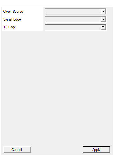
Set clock source for the TDC
Selects the clock source for the TDC counter. Available options: Board, Acquisition, 100MHz, 200MHz, 250MHz, 500MHz, External.Default: Board
Options: Board Acquisition 100MHz 200MHz 250MHz 500MHz External
Set the EDGE of the input signal used to trigger the TDC
Selects which edge of the input signal triggers timestamp capture. Options: Rising, Falling.Default: Rising
Options: Rising Falling
Set the EDGE of the T0 used to reset the TDC
Selects which edge of the T0 signal resets the counter. Options: Rising, Falling.Default: Rising
Options: Rising Falling
Usage
Functional overview
TDCSync operates with two clock domains:
- FAST_CLK: High-frequency clock driving the timestamp counter
- CLK: Output clock domain for data readout
The architecture consists of:
| Block | Function |
|---|---|
| 48-bit Counter | Free-running counter incremented at FAST_CLK rate |
| Edge Detector | Detects signal transitions based on configured polarity |
| Timestamp Latch | Captures counter value on input edge |
| CDC Handshake | Transfers timestamp safely across clock domains |
Operation
- The 48-bit counter runs continuously at the FAST_CLK frequency
- The counter can be reset to zero via the T0 input
- When the RUN signal is high, the counter increments
- On each detected edge of IN, the counter value is latched
- The latched value is transferred to the CLK domain via CDC logic
- DV pulses high when a valid timestamp is available on TIMESTAMP
Clock Domain Crossing
The block uses a Xilinx XPM CDC handshake primitive (xpm_cdc_handshake)
to safely transfer the 48-bit timestamp from the FAST_CLK domain to the
CLK domain. This ensures:
- No metastability issues
- No data corruption
- Proper synchronization
Maximum Event Rate
Due to the CDC handshake overhead, the maximum event rate is limited to:
$$ f_{\text{max}} = \frac{f_{\text{CLK}}}{4} $$
For a 125 MHz CLK, this corresponds to ~31 MHz maximum event rate.
Clock Source Options
The fast clock source can be configured via the Clock Source property:
| Option | Description |
|---|---|
| Board | Use the board’s default clock |
| Acquisition | Use the acquisition clock |
| 100MHz | Use internal 100 MHz clock |
| 200MHz | Use internal 200 MHz clock |
| 250MHz | Use internal 250 MHz clock |
| 500MHz | Use internal 500 MHz clock |
| External | Use external clock via CLKFAST pin |
Timing Resolution Examples
| Fast Clock | Resolution | Counter Overflow Time |
|---|---|---|
| 100 MHz | 10 ns | ~32 days |
| 200 MHz | 5 ns | ~16 days |
| 250 MHz | 4 ns | ~13 days |
| 500 MHz | 2 ns | ~6.5 days |