
Citiroc Trigger
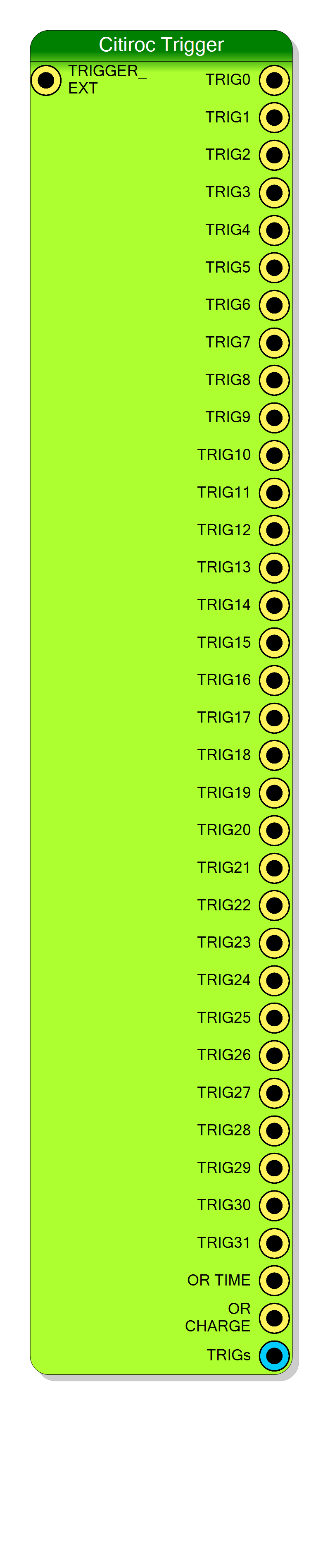
Access point to the 32 channel discriminator outputs of one CITIROC 1A ASIC on the DT5550W-Citiroc1A board, plus the two chip-level OR signals and the external trigger input of the chip. The block contains no logic at all: it only connects the board wrapper signals of the selected ASIC to nets in your design.
Introduction
Principle of Operation
Each CITIROC 1A channel has a fast discriminator whose output leaves the chip on its own pin. On the DT5550W-Citiroc1A the 32 outputs of every ASIC arrive at the FPGA as a 32-bit input bus, and the chip additionally provides two collective outputs and one external-trigger input.
This block is the door between those board-level signals and your schematic. It
instantiates nothing: CompileHDL emits only concurrent assignments of the form
<your net> <= A_TRIG0; -- for every connected output
TRIGGER_EXT_A_s <= <your net>(0); -- for the input
so there is no clock, no reset, no latency and no resource cost. Everything the block
exposes is combinational board wiring, and the ASIC property only selects which
prefix (A_, B_, C_, D_) those assignments use.
Pin Description
TRIG_EXT input pin. Leave it unconnected if you do not use external
triggering: no HDL is emitted and the board signal stays at '0'.
See the alert above about the pad type of this pin on the V1 block.
A_TRIG0 <= A_TRG(0) in the board wrapper, no mask, no register).
High while the channel’s trigger output is asserted.
Asynchronous to the design clock - resynchronise before use.
An unconnected output emits no HDL at all.
A_TRIG1 <= A_TRG(1) in the board wrapper, no mask, no register).
High while the channel’s trigger output is asserted.
Asynchronous to the design clock - resynchronise before use.
An unconnected output emits no HDL at all.
A_TRIG2 <= A_TRG(2) in the board wrapper, no mask, no register).
High while the channel’s trigger output is asserted.
Asynchronous to the design clock - resynchronise before use.
An unconnected output emits no HDL at all.
A_TRIG3 <= A_TRG(3) in the board wrapper, no mask, no register).
High while the channel’s trigger output is asserted.
Asynchronous to the design clock - resynchronise before use.
An unconnected output emits no HDL at all.
A_TRIG4 <= A_TRG(4) in the board wrapper, no mask, no register).
High while the channel’s trigger output is asserted.
Asynchronous to the design clock - resynchronise before use.
An unconnected output emits no HDL at all.
A_TRIG5 <= A_TRG(5) in the board wrapper, no mask, no register).
High while the channel’s trigger output is asserted.
Asynchronous to the design clock - resynchronise before use.
An unconnected output emits no HDL at all.
A_TRIG6 <= A_TRG(6) in the board wrapper, no mask, no register).
High while the channel’s trigger output is asserted.
Asynchronous to the design clock - resynchronise before use.
An unconnected output emits no HDL at all.
A_TRIG7 <= A_TRG(7) in the board wrapper, no mask, no register).
High while the channel’s trigger output is asserted.
Asynchronous to the design clock - resynchronise before use.
An unconnected output emits no HDL at all.
A_TRIG8 <= A_TRG(8) in the board wrapper, no mask, no register).
High while the channel’s trigger output is asserted.
Asynchronous to the design clock - resynchronise before use.
An unconnected output emits no HDL at all.
A_TRIG9 <= A_TRG(9) in the board wrapper, no mask, no register).
High while the channel’s trigger output is asserted.
Asynchronous to the design clock - resynchronise before use.
An unconnected output emits no HDL at all.
A_TRIG10 <= A_TRG(10) in the board wrapper, no mask, no register).
High while the channel’s trigger output is asserted.
Asynchronous to the design clock - resynchronise before use.
An unconnected output emits no HDL at all.
A_TRIG11 <= A_TRG(11) in the board wrapper, no mask, no register).
High while the channel’s trigger output is asserted.
Asynchronous to the design clock - resynchronise before use.
An unconnected output emits no HDL at all.
A_TRIG12 <= A_TRG(12) in the board wrapper, no mask, no register).
High while the channel’s trigger output is asserted.
Asynchronous to the design clock - resynchronise before use.
An unconnected output emits no HDL at all.
A_TRIG13 <= A_TRG(13) in the board wrapper, no mask, no register).
High while the channel’s trigger output is asserted.
Asynchronous to the design clock - resynchronise before use.
An unconnected output emits no HDL at all.
A_TRIG14 <= A_TRG(14) in the board wrapper, no mask, no register).
High while the channel’s trigger output is asserted.
Asynchronous to the design clock - resynchronise before use.
An unconnected output emits no HDL at all.
A_TRIG15 <= A_TRG(15) in the board wrapper, no mask, no register).
High while the channel’s trigger output is asserted.
Asynchronous to the design clock - resynchronise before use.
An unconnected output emits no HDL at all.
A_TRIG16 <= A_TRG(16) in the board wrapper, no mask, no register).
High while the channel’s trigger output is asserted.
Asynchronous to the design clock - resynchronise before use.
An unconnected output emits no HDL at all.
A_TRIG17 <= A_TRG(17) in the board wrapper, no mask, no register).
High while the channel’s trigger output is asserted.
Asynchronous to the design clock - resynchronise before use.
An unconnected output emits no HDL at all.
A_TRIG18 <= A_TRG(18) in the board wrapper, no mask, no register).
High while the channel’s trigger output is asserted.
Asynchronous to the design clock - resynchronise before use.
An unconnected output emits no HDL at all.
A_TRIG19 <= A_TRG(19) in the board wrapper, no mask, no register).
High while the channel’s trigger output is asserted.
Asynchronous to the design clock - resynchronise before use.
An unconnected output emits no HDL at all.
A_TRIG20 <= A_TRG(20) in the board wrapper, no mask, no register).
High while the channel’s trigger output is asserted.
Asynchronous to the design clock - resynchronise before use.
An unconnected output emits no HDL at all.
A_TRIG21 <= A_TRG(21) in the board wrapper, no mask, no register).
High while the channel’s trigger output is asserted.
Asynchronous to the design clock - resynchronise before use.
An unconnected output emits no HDL at all.
A_TRIG22 <= A_TRG(22) in the board wrapper, no mask, no register).
High while the channel’s trigger output is asserted.
Asynchronous to the design clock - resynchronise before use.
An unconnected output emits no HDL at all.
A_TRIG23 <= A_TRG(23) in the board wrapper, no mask, no register).
High while the channel’s trigger output is asserted.
Asynchronous to the design clock - resynchronise before use.
An unconnected output emits no HDL at all.
A_TRIG24 <= A_TRG(24) in the board wrapper, no mask, no register).
High while the channel’s trigger output is asserted.
Asynchronous to the design clock - resynchronise before use.
An unconnected output emits no HDL at all.
A_TRIG25 <= A_TRG(25) in the board wrapper, no mask, no register).
High while the channel’s trigger output is asserted.
Asynchronous to the design clock - resynchronise before use.
An unconnected output emits no HDL at all.
A_TRIG26 <= A_TRG(26) in the board wrapper, no mask, no register).
High while the channel’s trigger output is asserted.
Asynchronous to the design clock - resynchronise before use.
An unconnected output emits no HDL at all.
A_TRIG27 <= A_TRG(27) in the board wrapper, no mask, no register).
High while the channel’s trigger output is asserted.
Asynchronous to the design clock - resynchronise before use.
An unconnected output emits no HDL at all.
A_TRIG28 <= A_TRG(28) in the board wrapper, no mask, no register).
High while the channel’s trigger output is asserted.
Asynchronous to the design clock - resynchronise before use.
An unconnected output emits no HDL at all.
A_TRIG29 <= A_TRG(29) in the board wrapper, no mask, no register).
High while the channel’s trigger output is asserted.
Asynchronous to the design clock - resynchronise before use.
An unconnected output emits no HDL at all.
A_TRIG30 <= A_TRG(30) in the board wrapper, no mask, no register).
High while the channel’s trigger output is asserted.
Asynchronous to the design clock - resynchronise before use.
An unconnected output emits no HDL at all.
A_TRIG31 <= A_TRG(31) in the board wrapper, no mask, no register).
High while the channel’s trigger output is asserted.
Asynchronous to the design clock - resynchronise before use.
An unconnected output emits no HDL at all.
NOR32_TIME output pin of the
ASIC (A_OR_TIME(0) <= not A_NOR_TIME), so it is high while at least one channel’s
time discriminator fires. It is produced by the chip, not by the FPGA, and it is
not affected by any mask.
Asynchronous to the design clock.
OR32 charge output pin, passed straight through
(A_OR_CHARGE(0) <= A_OR32). High while at least one channel’s charge discriminator
fires.
Asynchronous to the design clock.
A_TRIGs <= A_TRG). Use it as a hit pattern to latch next to a readout frame.
Asynchronous to the design clock - latch it with the trigger that started the event,
not free-running.
Properties
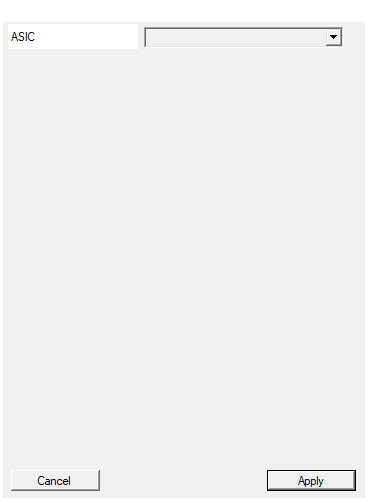
Select the ASIC to be connected to the Endpoint
Which of the four CITIROC sites on the board this block is wired to. It selects the prefix used in the generated assignments (A_TRIG0, B_TRIG0, …), so to read the
triggers of several ASICs you place one block per chip.
Valid values: A, B, C, D.
Default: A.
Default: A
Options: A B C D
Detailed Operation
What each output really is, on this board
The wiring below is taken from the DT5550W-Citiroc1A board wrapper
(dt5550w_top.vht). It is not the same as on the V2 board - see the comparison at
the end of this page.
| Symbol pin | Board wrapper expression | Origin |
|---|---|---|
TRIG0..TRIG31 |
A_TRIGn(0) <= A_TRG(n) |
the 32 discriminator pins of the ASIC, unmasked |
TRIGs |
A_TRIGs <= A_TRG |
the same 32 bits as one vector |
OR_TIME |
A_OR_TIME(0) <= not A_NOR_TIME |
the chip’s NOR32 time output, inverted in the FPGA |
OR_CHARGE |
A_OR_CHARGE(0) <= A_OR32 |
the chip’s OR32 charge output, straight through |
TRIGGER_EXT |
A_TRIG_EXT <= TRIGGER_EXT_A_s(0) |
an FPGA output pin that drives the chip’s external trigger input |
Note the asymmetry that the pin names hide: on this board OR_TIME is derived by
inverting the chip’s NOR output, while OR_CHARGE is the chip’s OR output used as it
comes. Both are chip-level signals, not an OR computed in the FPGA.
Emitted HDL
For every connected output pin the compiler appends one line to the architecture
body; unconnected pins are skipped entirely, so leaving TRIGs or the 32 individual
TRIGn unused costs nothing. The same applies to the input: if TRIGGER_EXT is left
open, no assignment is emitted and the board signal keeps its declared default "0".
Typical use
- Per-channel counting / rate meters - one counter per
TRIGn, after a synchroniser. - Event trigger -
OR_TIMEorOR_CHARGEinto a Monostable to build a clean, single-cycle trigger strobe for the Citiroc Analog readout block. - Channel pattern -
TRIGsas the 32-bit hit pattern latched together with a readout, to record which channels fired. - Forcing an acquisition - drive
TRIGGER_EXTfrom your own logic (a pulser, a coincidence with another board) to trigger the chip externally.
Differences with Citiroc Trigger - V2
The V2 block is a separate component for the DT5550W-Citiroc1A-V2 board; the two are not interchangeable, each one only appears on its own board.
| Citiroc Trigger (this block) | Citiroc Trigger - V2 | |
|---|---|---|
| Board | DT5550W-Citiroc1A | DT5550W-Citiroc1A-V2 |
| Pins | 36 | 39 |
| Extra pins | - | NOR_TIME, NOR_CHARGE outputs and a 32-bit MASK input |
TRIGn / TRIGs |
raw A_TRG |
A_TRG and not MASK - masked in the FPGA |
OR_TIME |
not A_NOR_TIME (chip pin, inverted) |
or_reduce(TRIGs) - the OR of the masked channels, computed in the FPGA |
OR_CHARGE |
A_OR32 |
A_OR32 (identical) |
TRIGGER_EXT pad type |
std_logic |
std_logic_vector |
Everything else - the ASIC property, the absence of clock/reset/logic, the version
string 1.1.0.0 - is identical.
Resources & Timing
-
Latency: None - the block emits concurrent assignments only, no register and no clock
-
Throughput: Not applicable
- No VHDL file is written to
pcores/and no logic is inferred; the cost of the block is zero. - Only available on the DT5550W-Citiroc1A board (board GUID
97567308-DA16-4E48-BB5E-ACE3E84DF06D). - Not available inside a subpage and not available in a state machine.