
ALU - GATED INTEGRATOR
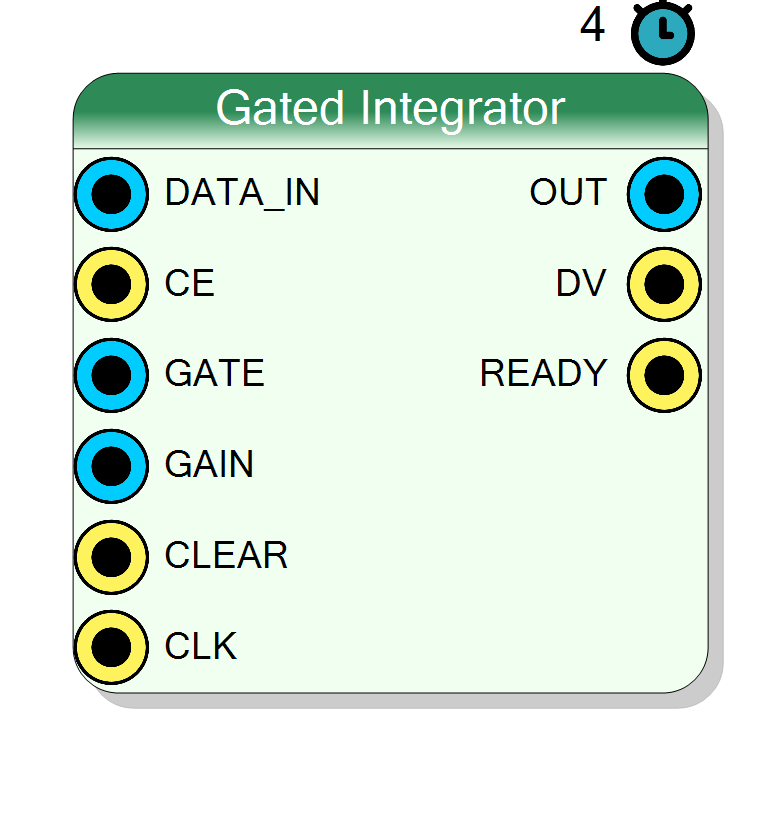
Gated accumulator with programmable integration window and gain. Accumulates input samples over a specified gate length, applies gain scaling, and outputs the integrated result. Features ready signal for external synchronization and clear function for reset. Optimized for pulse integration in nuclear physics and particle detection.
Introduction
The Gated Integrator accumulates input samples over a programmable time window (gate length), multiplies by a gain factor, and produces a single output value:
$$ \mathrm{OUT} = \mathrm{GAIN} \times \sum_{i=0}^{G-1} \mathrm{IN}[i] $$
where G is the gate length. This is commonly used in nuclear instrumentation
for charge integration, energy measurement, and pulse-height analysis.
The block includes handshake signals (DV_OUT, READY) for synchronization
with downstream processing stages.
Pin Description
DV_OUT is high.
Functional description
The gated integrator performs windowed accumulation followed by gain scaling:
- Accumulation phase: Sums
GATEconsecutive input samples - Scaling phase: Multiplies accumulated sum by
GAIN - Output phase: Asserts
DV_OUTand presents result onOUT
Operation modes
- Continuous: Automatically starts new integration after each cycle
- Triggered: External trigger controls integration start (via
CE) - Clear:
CLEARsignal resets accumulator immediately
Fixed-point arithmetic
All inputs and outputs use 32-bit signed fixed-point format:
DATA_IN: Input samples (32 bits, signed)GAIN: Scaling factor (32 bits, signed, typically Q16.16 format)OUT: Integrated and scaled result (32 bits, signed)
Handshake protocol
CE: Clock enable / trigger inputDV_OUT: Data valid output (high for one cycle when result ready)READY: Ready for new integration (high when idle)
Latency
Fixed latency of 4 clock cycles from gate completion to output valid.
Typical use cases
- Charge integration in PMT and SiPM readout
- Energy measurement in gamma spectroscopy
- Pulse-height analysis in nuclear physics
- Shaping amplifier replacement in digital systems