
Petiroc Digital
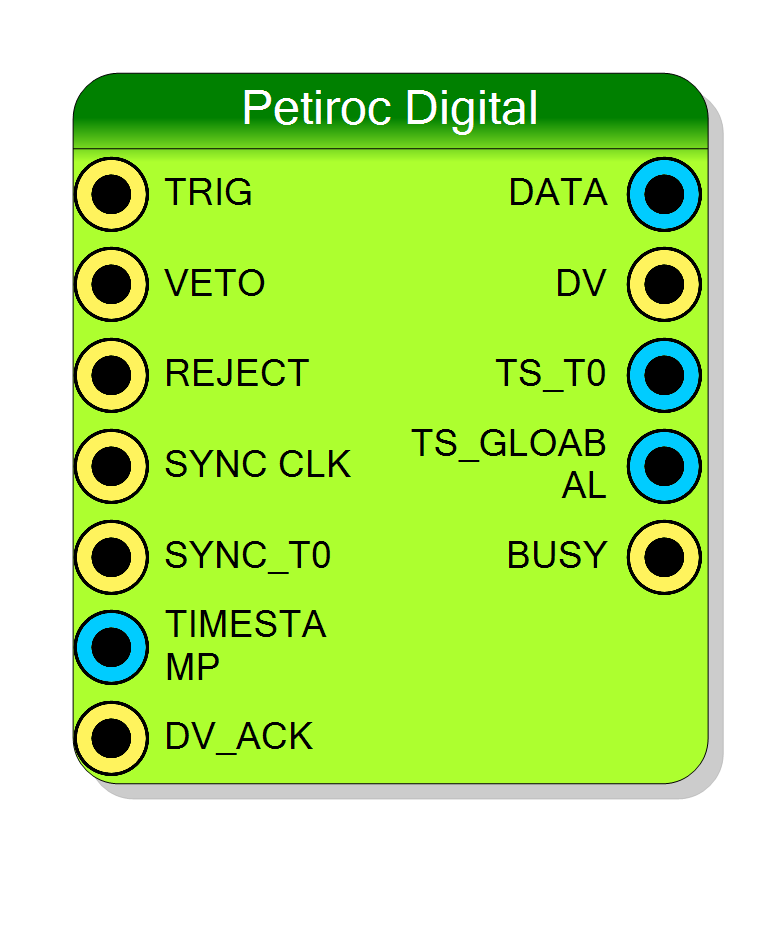
Digital readout engine for one PETIROC-2A on the DT5550W. On a trigger it fires the ASIC conversion (START_CONV), deserialises the LVDS data stream the chip sends back, packs it into 32 words of 32 bits, tags it with a local T0 counter and a 64-bit run timestamp, and then runs the channel-reset sequence that arms the ASIC for the next event.
Introduction
Principle of Operation
The PETIROC-2A digitises, inside the chip, both the charge and the time of every channel and then streams the whole 32-channel result out on a single serial LVDS line. This block is the FPGA half of that handshake. It
- waits for a trigger while the ASIC is idle,
- waits 16 clock cycles for the shaper to peak, then pulses START_CONV,
- watches the ASIC’s
TRANSMIT_ONline: while it is low the chip is shifting data out, and the block samples the serial line, - packs the bit stream into a 1024-bit
DATA_WORDvector, - raises DV, latches the two timestamps, and replays the
RAZ_CHN/VAL_EVTreset sequence so the analogue memories are clean for the next event.
The block never interprets the bits it receives: the meaning of the 960 data bits (10-bit Gray-coded fine time, charge and hit flags per channel) is applied later, by the host-side decoder shipped with Petiroc Frame Transfer.
Two timestamps, two clock domains
Two independent time references travel with each event:
TS_T0– a free-running 32-bit counter that this block maintains itself, in theSYNC_CLKdomain, and thatSYNC_T0resets. It measures time since the last sync pulse, so it is common to all boards that share the sameSYNC_T0distribution.TS_GLOABAL– the 64-bit value present on theTIMESTAMPinput, normally the design’s run timer.
Both cross into the readout clock domain through four-stage
xpm_cdc_array_single synchronisers, so SYNC_CLK may genuinely be a
different clock from the design clock. When you leave SYNC_CLK open the
compiler ties it to the project’s global clock and the two domains coincide.
Pin Description
TRIG is high and the ASIC’s TRANSMIT_ON is high. After an
event the machine waits in state x"2" until TRIG returns low, so a
permanently-high trigger yields exactly one event, not a burst. Usually
driven from OR_TIME of the Petiroc Trigger block.
daq_veto, which the
architecture never reads. Connecting it changes nothing - see the alert in
the description.
DV, forces the state machine
back to idle and restarts the RAZ_CHN / VAL_EVT channel-reset
sequence. Checked every clock, outside the state machine, so it overrides
whatever state the readout is in. Use it to drop an event that downstream
logic has decided not to keep (pile-up, out-of-window coincidence), which
also cleans the ASIC faster than waiting for the readout to finish.
SYNC_CLK edge. Pulse it once per run (or once
per accelerator/laser cycle) to give every board a common time origin.
Sampled in the SYNC_CLK domain, so it must be synchronous to that clock.
TS_GLOABAL with the event.
Because it goes through a 4-stage vector synchroniser (not a Gray-coded
one), connect a counter that is stable when sampled, or accept a few LSBs
of jitter on a fast-running counter.
DV. Drive it from the
ACK_x output of Petiroc Frame Transfer (or from your own consumer)
to close the handshake. If it is never asserted, DV stays high after the
first event and the consumer cannot tell events apart.
DV
and held until the next event. Word k occupies bits
32k+31 … 32k; inside a word bits 31..30 are the constant "00" inserted
by this block and bits 29..0 are 30 consecutive ASIC serial bits, the
first received in bit 29. Feed it unchanged to DATA_x of Petiroc
Frame Transfer; the field layout is applied on the host.
TRANSMIT_ON
(end of transmission), at the same clock as DATA_WORD, TS_T0 and
TS_GLOABAL are updated. It is a level, not a pulse: it stays high
until DV_ACK or REJECT clears it.
START_CONV is asserted, i.e. the conversion time referred to
the last SYNC_T0 pulse. Published with DV.
TIMESTAMP input captured at the
instant the trigger was accepted, published with DV. (The pin name is
spelled TS_GLOABAL in the component; it is kept verbatim here because
that is the name the schematic uses.)
TRANSMIT_ON is low in idle.
Count its high time to measure the live-time fraction of the run.
Properties
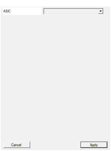
Select the ASIC to be connected to the Endpoint
Selects the PETIROC-2A this readout engine is bound to. It is pasted into
the board-support signal names emitted by CompileHDL:
PETIROC_<ASIC>_TRANSMIT_ON_s, PETIROC_<ASIC>_DATA_IN_s,
<ASIC>_START_CONV_s, <ASIC>_RAZ_CHN_s, <ASIC>_VAL_EVT_s.
| Value | Signals driven / read |
|---|---|
A |
PETIROC_A_*, A_START_CONV_s, A_RAZ_CHN_s, A_VAL_EVT_s |
B |
PETIROC_B_*, B_* |
C |
PETIROC_C_*, C_* |
D |
PETIROC_D_*, D_* |
Hidden (isVisible = False): the board plug-in sets it when the block is
placed. Note that Petiroc Analog drives RAZ_CHN and VAL_EVT of the
same chip too - do not place both blocks on the same ASIC letter, they
would fight over those two signals.
Default: A
Default: A
Options: A B C D
⚙️ Detailed Operation
State machine
┌────────────────────────────────────────────────────────┐
│ │
▼ │
┌─────────┐ TRANSMIT_ON=1 and TRIG=1 ┌─────────┐ │
│ x"0" │ ─────────────────────────► │ x"F" │ │
│ IDLE │ capture TIMESTAMP │ wait 16 │ │
│ BUSY=0 │ timeout := 4000 │ clocks │ │
└─────────┘ └────┬────┘ │
▲ │ START_CONV=1 │
│ │ (63 clocks) │
│ │ capture T0 │
│ ▼ │
│ timeout expired ┌────────────────────┐ │
├─────────────────────────────│ x"1" │ │
│ │ deserialise while │ │
│ │ TRANSMIT_ON = 0 │ │
│ └─────────┬──────────┘ │
│ │ TRANSMIT_ON 0→1│
│ │ DV=1, publish │
│ ┌─────────▼──────────┐ │
└─────────────────────────────│ x"2" wait TRIG=0 │─────┘
└────────────────────┘
Idle (x"0"). BUSY is low only here. The block refuses to start while
TRANSMIT_ON is low - if the ASIC is still shifting out a previous event the
block raises BUSY and waits. TRIG is tested as a level
(TRG0_i = '1' after two synchroniser stages), not as an edge, so a trigger
that is still high when the previous readout ends starts a new one
immediately; state x"2" exists precisely to force TRIG back to '0'
before the next event can be accepted. The 64-bit TIMESTAMP is latched here,
at the trigger.
Conversion start (x"F"). 16 clock cycles of dead time (the comment in
the source reads “attendi lo shaper” - wait for the shaper), then
START_CONV is asserted and a counter loaded with 0x3F, which holds the
pulse high for 63 further clocks. The 32-bit T0 counter is captured on the
same clock as START_CONV rises, so TS_T0 marks the conversion instant, not
the trigger instant.
Deserialisation (x"1").
- The falling edge of
TRANSMIT_ONmarks the start of transmission: the bit counter and the word counter are cleared and the captured T0 is moved into the output staging register. - While
TRANSMIT_ONis low, the serial line is sampled every other clock (askipflag toggles each cycle). The maximum ASIC bit rate the block can follow is therefore half the design clock. - Bits go into a 30-bit shift register. Every 30 bits one 32-bit word is
written into the staging vector as
"00" & <30 bits>; the oldest of the 30 bits ends up in bit 29, the newest in bit 0. - The rising edge of
TRANSMIT_ONends the transmission:DVgoes high,DATA_WORD,TS_T0andTS_GLOABALare published, and the ASIC reset sequence is restarted. - A safety timeout: if the ASIC never starts transmitting within 4000 clock
cycles of the trigger, the machine returns to idle and the event is lost
silently (no error flag,
DVis not raised).
Word format produced here
DATA_WORD is 32 words of 32 bits, 1024 bits total, of which 960 bits are
real ASIC data:
| Word bits | Content |
|---|---|
| 31 … 30 | always "00" (padding inserted by this block) |
| 29 … 0 | 30 consecutive ASIC serial bits, first received in bit 29 |
Downstream, Petiroc Frame Transfer copies this vector verbatim into the
frame it sends to the host, and the host decoder re-cuts each word into three
10-bit fields ([29:20], [19:10], [9:0]) - 96 fields in total, which is
exactly 32 words x 30 bits / 10. That is the reason for the 30-bits-per-word
packing: it keeps the 10-bit ASIC fields byte-aligned inside 32-bit words
without any bit shuffling on the host.
The RAZ_CHN / VAL_EVT reset sequence
Both this block and Petiroc Analog drive the same three ASIC control
signals (START_CONV, RAZ_CHN, VAL_EVT) for the selected chip. After
reset, after every completed readout and on every REJECT, an 8-bit counter
is loaded with 0x1F and counts down, driving:
| Counter value | RAZ_CHN |
VAL_EVT |
|---|---|---|
0x1F (start) |
1 |
0 |
0x15 |
0 |
0 |
0x07 |
1 |
0 |
0x00 (stops here) |
1 |
1 |
i.e. a 14-clock low pulse on RAZ_CHN to clear the channel memories, then
VAL_EVT is raised 7 clocks later and stays high until the next event. The
source comment is explicit about why it exists: “procedura necessaria per
evitare rumore nelle misure successive” - without it the following
measurements are noisy.
Back-pressure
DV stays high until it is cleared. Two things clear it: DV_ACK (the
intended handshake - Petiroc Frame Transfer drives its ACK_x output back
into this pin) and REJECT. The block itself does not wait for the
acknowledge before accepting the next trigger, so if the consumer is slower
than the trigger rate the staging vector is overwritten. Use BUSY or the
consumer’s FULL to gate the trigger if that matters.
Typical wiring
Petiroc Trigger Petiroc Digital Petiroc Frame Transfer
┌───────────┐ ┌──────────────┐ ┌──────────────────┐
│ OR_TIME ├────────────►│ TRIG │ │ │
└───────────┘ │ DATA_WORD ├────────────►│ DATA_x │
Run timer ──────────────►│ TIMESTAMP │ │ │
Sync pulse ──────────────►│ SYNC_T0 │ TS_T0 ───►│ TS_T0_x │
│ │TS_GLOABAL ─►│ TS_x │
│ DV ├────────────►│ DV_x │
│ DV_ACK │◄────────────┤ ACK_x │
│ BUSY ├──► dead-time counter │
└──────────────┘ └──────────────────┘