
Citiroc Analog - TDC (V2)
Second-generation analog readout sequencer for one CITIROC 1A ASIC on the DT5550W-Citiroc1A-V2 board. It keeps the hold / shift-register / ADC readout of the V1 block and adds three things V1 has not: a 4-bit-fine TDC that timestamps the asynchronous trigger OR, a configurable external validation and veto protocol with a timeout, and trigger / validation counters plus a status FLAGS word that travel with the event into the frame.

Introduction
Principle of Operation
Like the V1 Citiroc Analog block, this component owns the analog readout sequence
of a single CITIROC 1A: it waits HOLD_TIME cycles after the trigger edge, closes the
HG/LG peak-detector hold, walks the ASIC charge shift register and digitises each slot
through the board ADC, and publishes the result as a serial stream, as 32 parallel
pin triplets and as a packed 1024-bit frame word.
Three mechanisms are added on top.
1 — Time-to-digital conversion. The block instantiates tdc_sync_nofifo, fed by the
board’s six-phase TDC clock group. The asynchronous 32-channel trigger OR (T_OR32) is
captured on four skewed clocks plus the in-phase and quadrature system clocks, giving a
4-bit fine time inside one clock period (16 steps). The event timestamp is then
$$ t_{\mathrm{event}} ;=; \underbrace{\mathrm{coarse}}{44\ \mathrm{bits}} \times 16 ;+; \underbrace{\mathrm{fine}}{4\ \mathrm{bits}} $$
and is published on TS_OUT, replacing the coarse value captured at the trigger edge.
2 — Validation. An external decision (a coincidence, a downstream veto, a software
gate) can confirm or discard an event after the hold has been closed but before
the expensive shift-register walk begins. The FSM parks in one state waiting for
VALIDATION_IN; if the confirmation does not arrive within a programmable timeout the
event is either read out anyway or aborted, depending on the CFG register.
3 — Bookkeeping. A trigger counter, a validation counter and a 32-bit FLAGS word
that records why the event was released are exported as pins, so the Citiroc Frame
Transfer V2 block can append them to every packet.
Pin Description
TS_OUT at the
trigger edge before the TDC result arrives.
TS0_OUT at the trigger edge.
CNT_TRIGGER.
P_DV / P_FRAME_DV is produced.
P_FRAME_DV. Drive from ACK_x of the Citiroc Frame
Transfer V2 block; unconnected, P_FRAME_DV latches high permanently.
t_ref flag, marking
hits that coincide with the reference. Tie low if no external T0 is used.
CFG bit 4. A pulse arriving with no event in flight takes
the forced-frame path when CFG bit 2 is set and VETO is low. Ignored entirely
when CFG bit 0 is 0.
CNT_TRIGGER and CNT_VAL. Pulse it at the
start of every acquisition run so the counters in the packets start from zero.
TS0_IN frozen at the trigger edge, no TDC applied.
S_DV is high.
S_ENERGY_HG.
P_E_HG_n or P_FRAME_DATA.
CHARGE_HIT discriminator captured for that channel and
re-aligned through the internal HITMEM buffer to match the delayed sampling point.
Valid while S_DV is high.
P_DV.
P_DV.
FLAGS = 3), where the pins keep their
previous contents.
[31:29]=000, [28]=HIT, [27:14]=LG,
[13:0]=HG. Connect to DATA_x of the Citiroc Frame Transfer V2 block, which
serialises it LSW-first — so channel 31 reaches the PC first.
P_FRAME_ACK.
SCLK – copy of the ASIC shift-register clock driven by this block.
SR_IN – copy of the token bit injected into the ASIC shift register.
TRIG rising edges since the last
RUNRESET, published at the moment the trigger is accepted. Wire it to
CNT_TRIGGER_x of the Citiroc Frame Transfer V2 block so it is embedded in every
packet.
RUNRESET. Forced to zero while validation is disabled (CFG bit 0 = 0). Wire it
to CNT_VAL_x of the Citiroc Frame Transfer V2 block.
0 = validation disabled, 1 = validated, 2 = validation
timeout, 3 = forced frame. Level output, stable until the next decision. Wire it
to FLAGS_x of the Citiroc Frame Transfer V2 block.
Properties
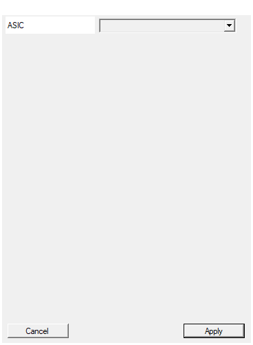
Select the ASIC to be connected to the Endpoint
Selects which of the four CITIROC 1A chips this instance drives. It changes no pin;
it renames the board nets the block binds to (Citiroc_<ASIC>_ADC_ENERGY_HG/LG,
Citiroc_<ASIC>_CHARGE_HIT_s, Citiroc_<ASIC>_SRIN_s, Citiroc_<ASIC>_SCLK_s,
Citiroc_<ASIC>_RESET_READ_s, <ASIC>_VAL_EVT_s, <ASIC>_RAZ_CHN_s,
<ASIC>_HOLD_HG_s, <ASIC>_HOLD_LG_s).
| Value | ASIC |
|---|---|
A |
chip A |
B |
chip B |
C |
chip C |
D |
chip D |
Two instances must never carry the same value. This is the only property of the
block — unlike V1 there is no readout-frequency setting, CLKDIV is fixed at 25 in
CompileHDL. The property is flagged isVisible = False in the component
definition, so it is not shown in the standard property dialog.
Default: A
Default: A
Options: A B C D
⚙️ Detailed Operation
Emitted HDL
CompileHDL writes two files into pcores/:
| File written | From embedded resource |
|---|---|
CitirocAnalogReadoutV2.vhd (entity CITIROCAnalogReadoutV2) |
CitirocAnalogReadout_NEW.vhd |
tdc_sync_nofifo.vhd |
tdc_sync_nofifo.vhd |
and instantiates the top entity with one generic:
| Generic | Value written by the compiler |
|---|---|
CLKDIV |
25, hard-coded |
V1’s ReadoutFrequency combo box is gone (it is commented out in the component source).
One shift-register step costs 2·(CLKDIV+1) = 52 clock cycles, so on the 160 MHz global
clock of the DT5550W-Citiroc1A-V2 the ASIC shift clock runs at roughly 3.1 MHz —
more than an order of magnitude faster than V1’s default.
Besides the pins, the block binds one extra internal board bus that is not drawn on the
canvas: TDC_CLOCKS ← TDC_SYNC_CLK (6 bits). Bit 0 is the system clock, bit 1 its
90°-shifted copy, bits 5:2 the four skewed fast clocks. Those come from the board’s
dedicated TDC PLL and cannot be rewired from the schematic.
What changed in the analog datapath
V1 (Citiroc Analog) |
V2 (this block) | |
|---|---|---|
| Boxcar filter length | 32 taps | 8 taps (16-entry shift register, tap0 − tap8) |
| Accumulator | 24 bit, result = bits [20:5] | 32 bit, result = bits [18:3] |
| Rounding | truncation | round to nearest (adds 1 when accumulator bit 2 is set) |
| ADC sampled | in the SCLK-high state, at the end of the count | mid-phase, at counter = CLKDIV/2 + 1 |
| Shift-register slots walked | 35 | 37 |
| First slots discarded | none | 3 (I > 2 guard) |
| Channel index | the slot number | separate CH_IDX, decoupled from the slot |
| Chip temperature | slot 32 | CH_IDX = 32 |
| Charge-SR reset pulse | 5 cycles | 17 cycles |
The shorter, rounded filter and the mid-phase sampling point are deliberate: the in-source comment states the sampling instant was chosen empirically with a logic analyser to land in the middle of the settled ADC output, and that the first three slots are skipped to absorb the ADC pipeline latency. The result is lower INL at a much higher shift rate.
Validation protocol
After the hold is closed (state 2) the FSM consults CFG (the VALIDATION_REG port):
flowchart TD
A[hold closed] --> B{CFG bit 0}
B -- 0 --> C["read out immediately<br/>FLAGS = 0x00000000<br/>CNT_VAL = 0"]
B -- 1 --> D{validation latched?}
D -- yes --> E["read out<br/>FLAGS = 0x00000001"]
D -- no --> F{timeout expired?}
F -- no --> D
F -- yes --> G{CFG bit 1}
G -- 0 --> H["read out anyway<br/>FLAGS = 0x00000002"]
G -- 1 --> I["abort event, reset ASIC<br/>FLAGS = 0x00000002"]
A validation pulse arriving while no event is in flight is handled separately: if
CFG bit 2 is set and VETO is low, the block re-issues P_DV and P_FRAME_DV with
the buffer it already holds and tags the event FLAGS = 0x00000003. This is the
“unsolicited / externally forced frame” path — it does not perform a new analog
readout, it republishes the previous one.
CFG register map (the VALIDATION_REG port)
| Bits | Name | Meaning |
|---|---|---|
| 0 | Validation enable | 0 = read out every trigger immediately (V1 behaviour). 1 = wait for VALIDATION_IN. |
| 1 | Timeout action | 0 = on timeout read the event out anyway. 1 = on timeout abort the event and reset the ASIC. |
| 2 | Forced-frame enable | 1 = a validation pulse with no event in flight republishes the last buffer (FLAGS = 3), gated by VETO. |
| 4 | Validation sensitivity | 0 = level sensitive on VALIDATION_IN. 1 = rising-edge sensitive. |
| 31:16 | Validation timeout | 16-bit countdown, preloaded at every accepted trigger, decremented one per clock. |
Bits 3 and 15:5 are not decoded by the HDL.
FLAGS output values
| Value | Meaning |
|---|---|
0x00000000 |
Validation disabled — the event was read out unconditionally. |
0x00000001 |
Validated: VALIDATION_IN arrived in time. |
0x00000002 |
Validation timeout. Whether data follows depends on CFG[1]. |
0x00000003 |
Forced frame: a validation arrived with no event in flight and CFG[2] = 1, VETO = 0. |
FLAGS is a level output, updated when the decision is taken and stable until the next
event — which is what makes it safe to sample it in the frame builder.
Counters
CNT_TRIGGER— total accepted trigger edges. Incremented on everyTRIGrising edge (including events later aborted), and published at the moment the trigger is accepted.CNT_VAL— total validation pulses seen. Published when the validation decision is taken; forced to0x00000000when validation is disabled.- Both are cleared by
RUNRESET, which is the natural “start of run” strobe.
Because CNT_TRIGGER counts triggers and the frame counter inside the Frame Transfer
block counts transmitted packets, comparing the two on the host gives the exact number
of events lost to vetoes, timeouts and FIFO back-pressure.
TDC path in detail
T_OR32 (asynchronous) ─┬─► rising-edge capture of {clk, clk90, sclk[3:0]} ─► fine[3:0]
└─► synchroniser (rising + falling edge FSMs) ─► coarse capture
T0 ───────────────────────► t_ref, latched with the hit
TS_IN[43:0] ──────────────► abstime (coarse)
│
▼
evnt_absolute_time[47:0] = coarse[43:0] & fine[3:0]
- The TDC is instantiated with
TS_BITS = 44andTOT_BITS = 9; only the timestamp is used, the time-over-threshold output is left open. - It carries a hold-off of 10 TDC clock cycles after each accepted hit
(
holdoff_timeis hard-wired tox"000A"inside the core), during which a second hit is not timestamped. - On the accepted trigger edge the FSM first writes the coarse value
TS_OUT <= TS_IN(59:0) & "0000"— the coarse counter shifted left by 4 so that it shares the LSB weight of the TDC — and arms a capture. When the TDC reports a valid measurement,TS_OUTis overwritten with"0000" & x"000" & TDC_TS(47:0). TS0_OUTis always the plain latchedTS0_IN, unchanged from V1.
The fine field is 1/16 of the TDC reference clock period. The absolute picosecond value
depends on which frequency the board PLL delivers on TDC_SYNC_CLK and is not
determined from the sources read here (the core’s own comments and the PLL instance
name suggest a 0.5 ns target, while the board model declares a 160 MHz global clock —
measure it rather than assuming).
T_OR32 must stay asynchronous
T_OR32 is wired to the TDC’s hit_asyn input and is sampled by clock-edge capture on
six different phases. Feeding it a signal that has already been registered in the system
clock domain destroys the fine-time information — the fine field will lock to one value.
Drive it from the ASIC trigger OR directly.
Resources & Timing
-
Latency: Trigger edge to
P_DV≈ HOLD_TIME + validation wait + 37·52 clock cycles (≈1900 clocks ≈ 12 µs of shift-register walk at 160 MHz) -
Throughput: One event per readout cycle;
BUSYcovers the whole cycle including the validation wait
- Emits
pcores/CitirocAnalogReadoutV2.vhdfrom theCitirocAnalogReadout_NEW.vhdresource, pluspcores/tdc_sync_nofifo.vhd. V1 emits only the plainCitirocAnalogReadout.vhdand no TDC. CLKDIVis hard-coded to 25 (V1 derives it from theReadoutFrequencyproperty).- The frame word layout is byte-for-byte the same as V1; what changed is what the Frame Transfer V2 block appends after it.
- Extra board binding not visible as a pin:
TDC_CLOCKS←TDC_SYNC_CLK(6 bits). - No memory-mapped registers and no SDK code —
CompileMMCandCompileSDKare empty. - Supported board: DT5550W-Citiroc1A-V2 (
26E86B08-6FEF-4B0F-8872-793CC478DA97). Not available inside subpages or state machines.