
Trigger LE
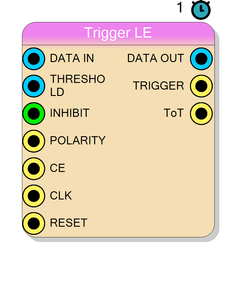
Leading-edge digital trigger with programmable word width, moving-average noise filtering and selectable output delay. Generates a single-cycle trigger pulse and a time-over-threshold (ToT) flag when the filtered input crosses a programmable threshold, with optional dead-time inhibition between successive triggers.
Introduction
The Trigger LE core implements a leading-edge discriminator commonly used in nuclear and high-energy physics data-acquisition chains.
Each clock cycle the input sample is optionally averaged over N samples (noise filter) and stored in a delay line of D samples.
A trigger is asserted when the filtered value crosses the user threshold with the selected polarity; the assertion starts the ToT signal that remains high as long as the condition is true.
To avoid re-triggering on the same pulse, an inhibition counter disables new triggers for a programmable number of clock cycles.
Pin Description
Width is set by WordSize (default 16).
The sample is first fed to the optional moving-average filter, then to the discriminator and delay line.
V_{thr} with the same bit-width as DATA_IN.When
POLARITY=1, a trigger occurs for $\tilde{x}[n]\ge V_{thr}$;when
POLARITY=0, for $\tilde{x}[n]\le V_{thr}$.
TRIGGER pulse (dead-time).Set to 0 for no inhibition.
Selects trigger edge polarity.
1– detect positive excursions above the threshold0– detect negative excursions below the threshold
Width = 1 bit.
The core processes data only when
CE=1; otherwise the internal state is frozen and outputs keep their last value except TRIGGER, which is forced low.
All internal operations are synchronous to the rising edge of
CLK.Recommended frequencies: 80 MHz (DT5550) or 50 MHz (V2495), but any frequency supported by timing closure is acceptable.
Clears delay line, filter accumulators, ToT state and inhibition counter.
DATA_OUT = \tilde{x}[n-D].Width equals WordSize.
Can be used to timestamp the leading edge or to start downstream processing.
Held high for as long as the trigger condition is satisfied, providing a coarse measurement of pulse width or charge.
Properties
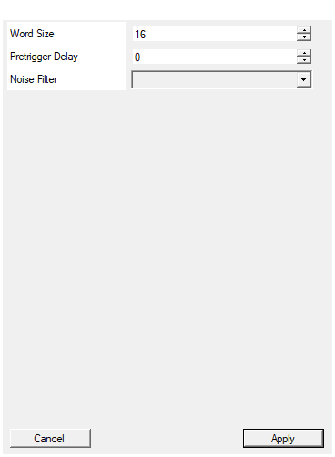
Set the number of bits of the data bus
Bit-width ofDATA_IN, THRESHOLD and DATA_OUT.A larger width increases dynamic range but consumes more FPGA logic and routing resources.
Acceptable range: 1 … 32, default 16.
Default: 16
Range: 2 – 64
Include programmable delay to embedd pretrigger logic in trigger module
Depth D of the output delay line (0 … 256).Determines the latency between
DATA_IN and DATA_OUT and allows alignment with other processing blocks.Increasing this value adds D registers to the design.
Default: 0
Range: 0 – 256
Specify the number of samples used in the moving average filter to reduce noise
Length N of the moving-average noise filter (power of two, 0 = disabled).Higher values improve signal-to-noise ratio as $10\log_{10}\N$ dB but increase latency and resource usage.
Internally implemented as a running sum with subtract-add logic and a right shift of $\log_2 N$.
Default: 0
Options: 0 2 4 8 16 32 64
Usage
Functional overview
Let
x[n]be the digitised input sample at clock nN– noise_filter (power of two)D– DataDelayV_{thr}– thresholdp– polarity bit (1= positive edge,0= negative edge)
Moving-average filter
$$ \tilde{x}[n] ;=; \frac{1}{N},\sum_{k=0}^{N-1} x[n-k] $$
Trigger decision
$$ \text{ToT}[n] ;=; \begin{cases} 1 & \text{if } \bigl(p=1 \land \tilde{x}[n]\ge V_{thr}\bigr) ;\lor; \bigl(p=0 \land \tilde{x}[n]\le V_{thr}\bigr) \ 0 & \text{otherwise} \end{cases} $$
The rising edge of ToT produces a single-cycle pulse TRIGGER.
After each pulse, new triggers are inhibited for INHIBIT cycles.
Delay line
$$ y[n] = \tilde{x}[n-D] $$
where y[n] is provided on DATA_OUT and D compensate the trigger delay to align the DATA_OUT with TRIGGER and ToT.
Timing
TRIGGERandToTare issued 1 clock cycle after the threshold comparison that satisfies the trigger condition.DATA_OUTis the filtered input delayed by D = DataDelay clock cycles.- Additional combinational delay is negligible; all paths are fully synchronous to
CLK.
Typical applications
- Photon or particle counting with scintillators and SiPM/PMT front-ends
- Leading-edge discriminator preceding a constant-fraction timing circuit
- Digital oscilloscope trigger with programmable dead-time