
DT5550W Board Controller
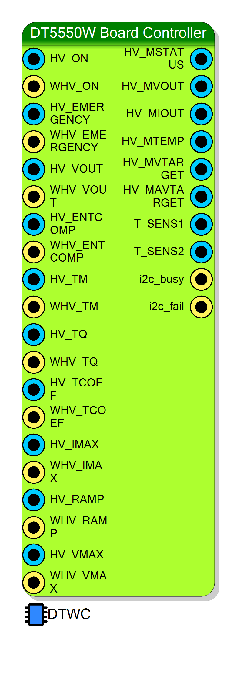
The single I2C housekeeping master of the DT5550W-Citiroc1A-V2 board. It owns the board I2C bus and, on its own initiative, reads the board-info EEPROM once at power-up, polls the two temperature sensors and continuously polls the A7585 high-voltage module, while accepting HV setting commands either from FPGA logic pins or from host registers.
Introduction
Principle of Operation
Everything that is not a detector signal on the DT5550W board hangs off one I2C bus: the HV module, two temperature sensors and the board identification EEPROM. This block is the only master on that bus. Place exactly one instance per design.
It is built from two pieces, both written into pcores/ at compile time:
DT5550W_iic.vhd- a sequencer that knows the register layout of each device;iic_master_andrea.vhd- a generic byte-level I2C master.
The sequencer never idles: whenever no command is pending it walks a housekeeping loop
power-up ──► read 16 bytes of board-info EEPROM (device 0x54) [once]
│
└──► every ~120 M clocks: read both temperature sensors (0x48, 0x4A)
└──► every ~20 M clocks : read 9 HV registers (0x73)
└──► otherwise : serve one pending HV/EEPROM write
and publishes the results on the monitor pins (or on the readout-bus registers, depending on Implementation mode). All timing is expressed in clock cycles of the project global clock; at the DT5550W default of 160 MHz the temperature refresh is about 0.75 s and the HV refresh about 0.13 s.
Pin Description
0x00:
'1' sends 0x00002710, '0' sends 0x00000000. The other 31 bits are ignored.
The write happens only when WHV_ON is strobed.
HV_ON. A single clock cycle at '1' is latched and served as
soon as the sequencer is free. Keep HV_ON stable until then.
0x00002710 to A7585 register 0x1F and ignores this pin’s value.
0x1F.
One clock cycle is enough; it is latched until served. Second in priority, right after
WHV_ON.
0x02 when WHV_VOUT is strobed. No scaling is applied by the block: the
value must already be in the module’s own number format.
HV_VOUT. One clock cycle, latched until served.
0x01: '1' sends 0x00004E20, '0' sends 0x00000000.
HV_ENTCOMP. One clock cycle, latched until served.
0x08 when
WHV_TM is strobed.
HV_TM. One clock cycle, latched until served.
0x09 when
WHV_TQ is strobed.
HV_TQ. One clock cycle, latched until served.
0x1C
when WHV_TCOEF is strobed.
HV_TCOEF. One clock cycle, latched until served.
0x06 when
WHV_IMAX is strobed.
HV_IMAX. One clock cycle, latched until served.
0x03 when WHV_RAMP is
strobed. Set it before enabling the output if you need a controlled ramp.
HV_RAMP. One clock cycle, latched until served.
0x04 when
WHV_VMAX is strobed. Lowest priority of the ten HV settings.
HV_VMAX. One clock cycle, latched until served.
HV status flags, rebuilt once per monitor scan:
- bit 0 - A7585 register
0x00is non-zero (output enabled); - bit 1 - register
0xF9is non-zero (voltage compliance); - bit 2 - register
0xFAis non-zero (current compliance).
Bits 3 to 31 are never driven - mask them out.
0xE7,
refreshed once per monitor scan (about every 20 M clock cycles).
0xE8,
refreshed once per monitor scan.
0xEA, refreshed
once per monitor scan. This is the HV module’s own sensor, not the two board sensors.
0xEB, refreshed once
per monitor scan.
0xEC, refreshed
once per monitor scan. Compare it with HV_MVTARGET to watch a ramp in progress.
0x48): the two bytes read from its
register 0x00, packed as x"00000" & byte0 & byte1(3 downto 0), so the useful field
is bits [11:0]. Refreshed about every 120 M clock cycles.
0x4A), same packing and same refresh rate
as T_SENS1.
DT5550W_iic.vhd. Leave it unconnected.
Properties
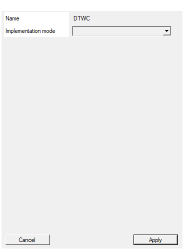
Set the name of the endpoint
Name of the readout-bus endpoint. Read-only: the compiler uses the fixed stringDTWC for the endpoint, for the register names (SCI_REG_DTWC_...) and for the HDL
signal names, whatever is displayed here.
Default: DTWC.
Default: DTWC
Select if map the register directly to the readout bus (memory mapped) or made available in the scicompiler logic
Where the HV settings and monitor values live.
| Value | Effect |
|---|---|
Logic |
30 pins on the symbol, HV driven by FPGA logic; the DTWC endpoint is created with no registers |
Memory Mapped |
no pins at all on the symbol; the same signals are bound to 10 write and 8 read registers of the DTWC endpoint and driven by the host |
Switching mode changes the symbol, so any wiring made in Logic mode is lost when you
switch to Memory Mapped.
Default: Logic.
Default: Logic
Options: Logic Memory Mapped
Detailed Operation
Devices on the bus
| 7-bit address | Device | What the block does with it |
|---|---|---|
0x73 |
A7585 high-voltage module | polls 9 registers, writes the 10 settings |
0x48 |
temperature sensor 1 | reads 2 bytes from register 0x00 |
0x4A |
temperature sensor 2 | reads 2 bytes from register 0x00 |
0x54 |
board-info EEPROM | reads 16 bytes at power-up, writes single bytes on request |
Every HV access is a fixed frame: the register address byte, then the constant byte
0x01 (the module’s data-format selector, commented fixed point data format in the
source), then four data bytes, least significant first - written for a setting, read
back for a monitor value.
Arbitration order
Inside the idle state the sequencer chooses, strictly in this order:
- the board-info EEPROM read, if it has never been done;
- the temperature scan, when its timer has expired;
- the HV monitor scan, when its timer has expired;
- one pending write, in the fixed priority
HV_ON>HV_EMERGENCY>HV_VOUT>HV_ENTCOMP>HV_TM>HV_TQ>HV_TCOEF>HV_IMAX>HV_RAMP>HV_VMAX> EEPROM byte write.
The two timers are only decremented in case 4, so a pending scan blocks all writes until it finishes, and the refresh periods quoted below are lower bounds, not guarantees.
HV settings (what each write really sends)
| Pin | A7585 register | Data sent |
|---|---|---|
HV_ON |
0x00 |
0x00002710 if bit 0 of the pin is '1', otherwise 0x00000000 |
HV_EMERGENCY |
0x1F |
always 0x00002710 - the pin value is ignored, only the strobe matters |
HV_VOUT |
0x02 |
the 32-bit pin value, unchanged |
HV_ENTCOMP |
0x01 |
0x00004E20 if bit 0 of the pin is '1', otherwise 0x00000000 |
HV_TM |
0x08 |
the 32-bit pin value, unchanged |
HV_TQ |
0x09 |
the 32-bit pin value, unchanged |
HV_TCOEF |
0x1C |
the 32-bit pin value, unchanged |
HV_IMAX |
0x06 |
the 32-bit pin value, unchanged |
HV_RAMP |
0x03 |
the 32-bit pin value, unchanged |
HV_VMAX |
0x04 |
the 32-bit pin value, unchanged |
The four “pass-through” cases send the raw 32 bits you provide: the block performs no scaling and no unit conversion, so the value must already be in the number format the HV module expects.
HV monitor scan
One pass of the scan reads nine registers and publishes the previous one’s result, so the values on the pins are always one step old inside a pass, and fully refreshed once per pass:
| A7585 register read | Published on |
|---|---|
0x00 |
HV_MSTATUS bit 0 - set when the register is non-zero (HV enabled) |
0xE7 |
HV_MVOUT - output voltage monitor |
0xE8 |
HV_MIOUT - output current monitor |
0xEA |
HV_MTEMP - module temperature |
0xEB |
HV_MVTARGET - voltage target |
0xEC |
HV_MAVTARGET - actual voltage target |
0xF9 |
HV_MSTATUS bit 1 - set when the register is non-zero (voltage compliance) |
0xFA |
HV_MSTATUS bit 2 - set when the register is non-zero (current compliance) |
0xFB |
discarded (the scan ends here and the timer is reloaded with 20 000 000 cycles) |
Only bits 0, 1 and 2 of HV_MSTATUS are ever driven; the remaining 29 bits are never
assigned. The six 32-bit monitor words are passed through exactly as they come off the
bus, low byte first.
Temperature sensors
Each sensor is read as two bytes from its register 0x00, and the result is published as
T_SENSn = x"00000" & byte0 & byte1(3 downto 0)
i.e. a 12-bit field in bits [11:0], the first byte received occupying bits [11:4].
Sensor 1 is the device at 0x48, sensor 2 the device at 0x4A. The timer is reloaded
with 120 000 000 clock cycles after both sensors have been read.
Board information (EEPROM)
At power-up the block reads 16 bytes from the EEPROM at 0x54 and splits them into four
board-level signals that the rest of the board framework consumes - they are not
symbol pins:
| Signal | Bytes | Content |
|---|---|---|
PGB_EEPROM_KEY |
0-3 | validity key |
PGB_REG_MODEL |
4-6 | board model, zero-extended to 32 bits |
PGB_ASIC_COUNT |
7 | number of ASICs, zero-extended to 32 bits |
PGB_BOARD_SN |
8-11 | board serial number |
A single EEPROM byte can also be written, but only from the board framework signals
REG_EEPROM_WR (data in bits [7:0], internal address in bits [15:8]) and
INT_EEPROM_WR; the block exposes no pin for it.
Status outputs
i2c_fail is the sticky OR of every missing acknowledge since reset: the sequencer
accumulates i2c_acks <= i2c_acks or not ack after each byte and never clears it except
on reset. Treat it as “at least one device did not answer since power-up”, not as an
instantaneous error.
Implementation mode
-
Logic (default) - every setting and every monitor value is a pin on the symbol, and the readout-bus endpoint
DTWCis created with no registers. The HV is driven by your FPGA logic. -
Memory Mapped - the symbol has no pins at all; the same signals are bound to the registers of the
DTWCendpoint instead, and the host drives the HV over the readout bus. The generated register list isRegister Access ON_OFF,HV_EMERGENCY,HV_SET_VOLTAGE,HV_ENABLE_TCOMP,HV_T_M,HV_T_Q,HV_TCOMP_COEF,HV_MAX_I,RAMP_SPEED,HV_MAX_Vwrite HV_STATUS,HV_OUTV,HV_IOUT,HV_TEMP,HV_VTARGET,HV_AVTARGET,TEMP_SENS_1,TEMP_SENS_2read exposed to the SDK as
SCI_REG_DTWC_<register>. In this mode the write strobes are the register-file write pulses themselves, so a single host write is enough. No C or Python helper is generated:CompileSDKemits only the JSON register description.
The endpoint name is fixed to DTWC - the Name property is read-only and the compiler hardcodes the same string.
Messages printed by the compiler
Generating HDL code For <designator>- informational.Generating memory mapped component: DTWC- informational.SDK starting code generation- informational.SDK address undefined for DTWC- error, the endpoint got no base address and the compilation stops.
Practical notes
- Bring the HV up through the module’s own ramp: set
HV_VMAX,HV_IMAXandHV_RAMPfirst, then the target withHV_VOUT, then assertHV_ON. HV_EMERGENCYis a one-shot: strobeWHV_EMERGENCYand the block writes the emergency register, whatever is on the data pin.- Poll
HV_MVOUT/HV_MSTATUSto follow the ramp; they refresh about every 20 M clock cycles. - Do not add another I2C master on the same bus.
Resources & Timing
-
Latency: Housekeeping driven: the board-info EEPROM is read once after reset; the temperature scan reloads a 120 000 000 cycle timer (~0.75 s at 160 MHz); the HV monitor scan reloads a 20 000 000 cycle timer (~0.13 s at 160 MHz). Both timers start at 125 000 000 cycles.
-
Throughput: One I2C transaction at a time on a bus clocked at clk/312 (~513 kHz at 160 MHz). A pending setting is served at the next idle visit, i.e. after the housekeeping transaction in progress.
- Instantiate exactly one of these blocks: it is the only master of the board I2C bus.
- Two VHDL files are written to
pcores/:DT5550W_iic.vhdandiic_master_andrea.vhd. PGB_EEPROM_KEY,PGB_REG_MODEL,PGB_BOARD_SN,PGB_ASIC_COUNT,REG_IIC_STATUS,REG_EEPROM_WRandINT_EEPROM_WRare wired to board-level signals of the same name and are not reachable from the schematic.- Available only on the DT5550W-Citiroc1A-V2 board (board GUID
26E86B08-6FEF-4B0F-8872-793CC478DA97); not available in a subpage or in a state machine.