
ADC Ready
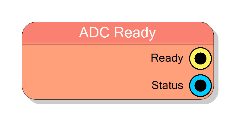
Board pin block that exposes the health of the four DT5550 ADC front ends: one Ready flag that rises when the SPI configuration sequence has completed, and a 12-bit Status word carrying the per-ADC bit-lock, initialised and SERDES delay-lock flags. Read-only, no logic of its own.
Introduction
Principle of Operation
The DT5550 carries four ADC devices feeding 32 analog channels. They are not usable the instant the FPGA comes out of reset: an on-board state machine must reset them, push a fixed SPI programming sequence into each one, train the SERDES bit alignment and lock the input delays. Only then do the sample buses carry meaningful numbers.
ADC Ready is the diagram-side window on that process. It gives you:
- Ready - one bit, high when the configuration sequence has finished;
- Status - twelve bits, the individual sub-flags that got it there.
Nothing in this block is a register you can write. It is a set of wires out
of the board’s ADC subsystem (adcs_top), synchronised into your clock
domain.
Pin Description
ADC configuration complete (canvas caption Ready).
'1' once the board’s ADC state machine has finished resetting and
programming all four ADCs; '0' from the moment the sequence restarts.
A level, not a pulse, and not a per-sample data-valid.
The assignment that drives this pad is emitted unconditionally -
unlike ADCSTATUS there is no unconnected-pad guard, so this pin must be
connected.
Per-ADC status flags (canvas caption Status). Twelve independent
bits: [3:0] bit-lock, [7:4] initialised, [11:8] SERDES delay lock,
one bit per ADC device 1 to 4 in each group. All-ones means all four
front ends are healthy.
Safe to leave unconnected - the plug-in checks the pad and simply omits the assignment.
Synchronised bit by bit into the readout clock domain, so do not compare it against an exact pattern on a single cycle.
Properties
adcs_top.
⚙️ Detailed Operation
What the block compiles to
CompileHDL adds two output pads and emits plain concurrent assignments:
<ready signal> <= ADC_READY; -- always emitted
<status signal> <= ADC_STATUS; -- emitted only if the pad is connected
Note the asymmetry: the ADCSTATUS assignment is wrapped in a
<> "open" guard, the ADCREADY assignment is not.
Where the signals come from
ADC_READY and ADC_STATUS are not part of the DT5550 top-level
template. They are declared by IstantiateAdc in the board plug-in:
signal ADC_READY : STD_LOGIC_VECTOR(0 downto 0);
signal ADC_STATUS : STD_LOGIC_VECTOR(11 downto 0);
together with the adcs_top instance that drives them.
The Status word, bit by bit
Inside adcs_top a 13-bit vector is assembled and then split - twelve bits
to ADC_STATUS, the thirteenth to ADC_READY:
| Bit | Meaning | ADC |
|---|---|---|
| 0 | bit_locked - serial word alignment found |
ADC 1 |
| 1 | bit_locked |
ADC 2 |
| 2 | bit_locked |
ADC 3 |
| 3 | bit_locked |
ADC 4 |
| 4 | initialized - device brought up |
ADC 1 |
| 5 | initialized |
ADC 2 |
| 6 | initialized |
ADC 3 |
| 7 | initialized |
ADC 4 |
| 8 | serdes_delaylock - input delay trained |
ADC 1 |
| 9 | serdes_delaylock |
ADC 2 |
| 10 | serdes_delaylock |
ADC 3 |
| 11 | serdes_delaylock |
ADC 4 |
Bit 12 of the internal vector is the same signal that comes out on the
Ready pin; it is not repeated inside ADC_STATUS.
A healthy, fully configured board therefore shows ADC_STATUS = x"FFF"
together with Ready = '1'.
How Ready behaves
ADC_READY is driven by the ADC configuration FSM in adcs_top:
- it is cleared (
'0') at the top of the sequence, together withadc_programmed <= '0'and the ADC reset assertion, and at the same point a watchdog is armed with a count of 25 000 000; - it is set (
'1') at the last step of the SPI programming sequence, where the watchdog is disarmed.
So Ready is a “configuration finished” flag, not a per-sample data-valid. It stays high for the whole run unless the sequence restarts.
Clock domain and coherency
All thirteen bits cross into your clock domain through one
xpm_cdc_array_single instance (DEST_SYNC_FF => 4, WIDTH => 13), with
dest_clk => READOUT_CLK - the same 80 MHz readout clock the ADC samples
are registered on.
Add four destination-side flip-flops’ worth of latency (DEST_SYNC_FF = 4)
to anything you time against these flags.
Typical use
- Gating the acquisition: hold your DAQ blocks disabled until
Ready = '1'. - Front-panel or software diagnostics: route
Statusto a readable register so the host can tell which ADC failed to lock. - Startup supervision: a
Readythat never rises points at the watchdog in the configuration FSM rather than at your own logic.
Board availability
Offered only on the DT5550 (board plug-in GUID
413F904B-7FD0-43EF-B127-74278C23F1A5).
SupportedBoard also lists DT5550SE and DT5560; neither has any effect.
The toolbox filter in Form1_plugins.vb implements a BOARD_MODELS.DT5550
branch only, no board plug-in declares itself DT5550SE, and the DT5560
board neither declares ADC_READY / ADC_STATUS nor has an IstantiateAdc
equivalent.
Resources & Timing
- Latency: Combinational in the block itself; the board adds a 4-flip-flop clock-domain synchroniser (
xpm_cdc_array_single,DEST_SYNC_FF = 4) on all 13 bits.
- No registers, no SciSDK endpoint, no resource cost of its own.
- Requires an Analog Input or AFE5550 block in the design; that is
what instantiates
adcs_topand declares the signals this block reads.