
Polarity Invert (TM)
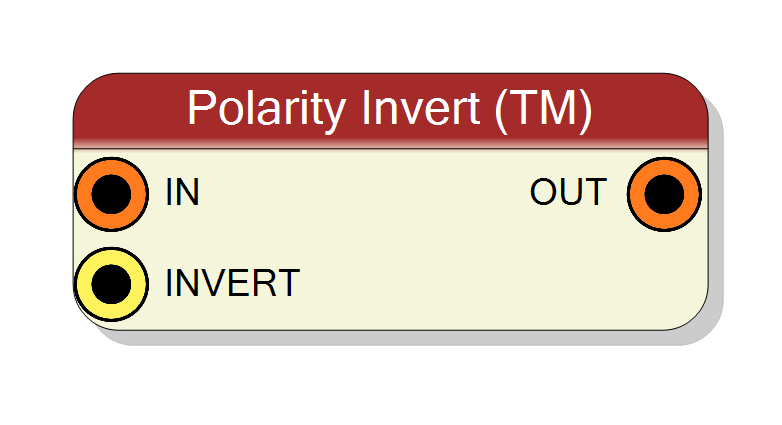
Time-multiplexed polarity inverter: the same switchable inversion as the scalar Polarity Invert, replicated over every lane of a TM bus. One shared INVERT bit controls all lanes. Purely combinational, zero latency. Unlike the scalar block, its SIGNED path sign-extends correctly when Effective # bits is smaller than Input bits.
Introduction
Principle of Operation
This is the time-multiplexed twin of Polarity Invert. A TM bus carries TM Factor consecutive samples side by side in one clock; this block instantiates one inverter per lane and applies the same operation to all of them in parallel, still with zero latency.
For every lane $i = 0 \ldots \mathrm{TM} - 1$, when INVERT = 1:
| Input sign | operation | in words |
|---|---|---|
UNSIGNED |
$y_i = (2^{N_{\rm eff}} - 1) - x_i$ | reflection about full scale — the bitwise complement |
SIGNED |
$y_i = -x_i \pmod{2^{N_{\rm eff}}}$ | two’s-complement negation |
and when INVERT = 0 every lane passes through (truncated to
$N_{\rm eff}$ = Effective # bits).
Lane layout
The bus is a plain concatenation and the lane pitch is Input bits, i.e.
the port width — not Effective # bits. For a TM factor of 4 and
Input bits = 16:
bit 63 48 47 32 31 16 15 0
┌────────────┬────────────┬────────────┬────────────┐
IN │ lane 3 │ lane 2 │ lane 1 │ lane 0 │
└────────────┴────────────┴────────────┴────────────┘
Lane $i$ occupies bits $[(i+1)\cdot A - 1 : i\cdot A]$ with $A$ = Input bits,
and OUT uses the identical layout. Inside each lane only the low
Effective # bits take part in the arithmetic. (This spacing is the subject of
the core’s own revision note, “Corrected TM spacing” — earlier revisions packed
the lanes at the effective width instead.)
One control for all lanes
INVERT is a single bit shared by every lane, and it is a scalar pin, not a
TM pin: there is no way to invert some lanes and not others. That is almost
always what you want, because the lanes of a TM bus are consecutive samples of
one detector channel, not different channels.
Pin Description
IN on the canvas). Input bits per lane × Time Mux
lanes, lane $i$ at bits $[(i+1)\cdot\text{Input bits}-1 : i\cdot\text{Input bits}]$.
Only the low Effective # bits of each lane take part in the arithmetic;
the rest are discarded.
Invert control (INVERT on the canvas), a single scalar bit shared
by every lane — this pin is not time-multiplexed.
- 0 → every lane passes through (truncated to Effective # bits)
- 1 → every lane is inverted, per Input sign
It has no default: drive it from a register or a constant.
OUT on the canvas), same width, same lane pitch and
same TM factor as IN. Valid in the same clock period — no pipeline
register. In SIGNED mode the per-lane result is sign-extended to the lane
pitch.
Properties
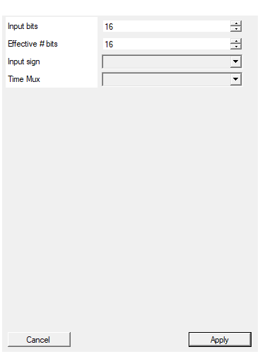
Set the number of bits of the input
Width in bits of one lane of IN and OUT; the total bus width is
Input bits × Time Mux. It is also the lane pitch used to slice the bus,
so it must match the pitch of whatever produces the TM stream.
Range: 2 to 2048. Changing it rebuilds the symbol.
Default: 16
Default: 16
Range: 2 – 2048
Set the effective number of significative bits in the data. For example for 14 bit ADC board set this number to 14
Effective # bits — the significant bits inside each lane, and the width
the inversion is computed in. Set it to the real ADC resolution so the
UNSIGNED reflection mirrors about the right full-scale value.
Must be ≤ Input bits (the core slices
a_slice(EffSize-1 downto 0); a larger value will not elaborate). Bits
above it are discarded in every lane.
Range: 2 to 2048.
Default: 16
Default: 16
Range: 2 – 2048
Select the sign/unsign of the input
How each lane is interpreted, and therefore what “invert” means.
| value | inversion | overflow behaviour | widening to lane pitch |
|---|---|---|---|
UNSIGNED |
$y = (2^{N_{\rm eff}}-1) - x$, i.e. bitwise NOT | cannot overflow | zero extension |
SIGNED |
$y = -x$ in two’s complement | $-2^{N_{\rm eff}-1}$ wraps onto itself | sign extension |
Fixed at synthesis; only INVERT is switchable at runtime.
Default: UNSIGNED
Default: UNSIGNED
Options: UNSIGNED SIGNED
Set number of samples for each clock cycle
Time Mux — the number of lanes carried per clock, i.e. how many inverter
instances are built and how wide IN / OUT are. It must match the TM
factor of the nets you connect.
Allowed: 2, 4, 8, 16, 32. Logic cost and total bus width scale linearly with it.
Default: 4
Default: 4
Options: 2 4 8 16 32
⚙️ Detailed Operation
Datapath
Resources/Code/polinvert_tm.vhd is a for … generate over TMFactor, with
one of two bodies selected at elaboration by the SIGN generic. Per lane:
a[(i+1)*A_SIZE-1 : i*A_SIZE] ──► slice to AN_SIZE bits ──► invert ──► resize to A_SIZE ──► b[...]
▲
INVERT ─────┘ (shared)
with A_SIZE = Input bits, AN_SIZE = Effective # bits, SIGN =
Input sign, TMFactor = Time Mux. There is no interaction of any kind
between lanes and no sequential element anywhere in the file: the whole block
is combinational.
INVERT= 1,UNSIGNED→A_MAX_UNSIGNED - a_slice, whereA_MAX_UNSIGNEDisAN_SIZEones. Subtracting from all-ones never borrows, so this is the bitwise NOT of the lane.INVERT= 1,SIGNED→0 - a_sliceinAN_SIZE-bit signed arithmetic.
The one thing people get wrong: the most negative value
As in the scalar block, the SIGNED negation is modulo $2^{N_{\rm eff}}$ and
is never clamped. The file declares A_MAX_SIGNED and A_MIN_SIGNED
constants but never reads them; there is no saturation logic.
$$ -2^{N_{\rm eff}-1} ;\longmapsto; 0 - \left(-2^{N_{\rm eff}-1}\right) \equiv -2^{N_{\rm eff}-1} $$
With Effective # bits = 16, a lane holding 0x8000 (−32768) comes out
holding 0x8000 — that lane is not inverted while all the others are.
Difference from the scalar block: sign extension
When Effective # bits is smaller than Input bits, the result has to be
widened back to the lane pitch. This block does it correctly for both modes:
the unsigned branch uses resize(unsigned(...), A_SIZE) and the signed branch
uses resize(signed(...), A_SIZE), so a negative result is sign-extended
into the unused top bits of its lane.
The scalar Polarity Invert zero-extends in both modes, which is wrong for
SIGNED with Effective # bits < Input bits. If you are moving a design
between the scalar and TM versions with that combination of settings, the two
will not produce the same numbers — the TM one is the one to trust.
Effective # bits truncates
Each lane is sliced to its low AN_SIZE bits before anything happens, so bits
above Effective # bits are discarded even when INVERT = 0. Set
Effective # bits to the real ADC resolution (14 for a 14-bit ADC carried in a
16-bit lane) so that the UNSIGNED reflection mirrors about $2^{14}-1$ rather
than about $2^{16}-1$. Effective # bits must be ≤ Input bits: a larger
value produces an out-of-range slice and the design will not elaborate.
Configuration
Input bits, Effective # bits, Input sign and Time Mux all become VHDL
generics and are fixed at synthesis. Only INVERT is live. Drive it from a
Register block to make the polarity software-selectable:
TM ADC bus ─────────► IN ┌──────────────────┐
│ Polarity Invert │──► OUT ──► TM shaper / TM trigger
Register (1 bit) ──► INVERT (TM) │
└──────────────────┘
The TM factor of IN and OUT is whatever Time Mux says, and the Sci-Compiler
editor will refuse to connect them to TM nets of a different factor.
Timing and cost
| quantity | value |
|---|---|
| latency | 0 clocks (combinational) |
| throughput | TM Factor samples per clock |
| clock / reset | none — no sequential elements |
| logic cost | TM Factor independent Effective # bits-wide subtract/mux pairs |
Cost grows linearly with Time Mux: 32 lanes of a 16-bit inverter is 32 copies
of the scalar logic. In UNSIGNED mode each copy reduces to a row of XOR gates
against the shared INVERT bit, which is very cheap; the SIGNED path needs a
real subtractor per lane and is where a wide, high-factor instance starts to
cost carry chains — and, being combinational, it lands entirely inside the
timing path of the surrounding registers.
Resources & Timing
-
Latency: 0 clocks — purely combinational, no clock or reset pin
-
Throughput: TM Factor samples per clock
- One Effective # bits-wide subtractor and multiplexer per lane; in
UNSIGNEDmode each degenerates to a row of XOR gates. - No memory-mapped registers are generated.
- The
SIGNEDpath here sign-extends to the lane pitch, whereas the scalar Polarity Invert zero-extends; the two agree only when Effective # bits = Input bits.