
Multi MUX TM
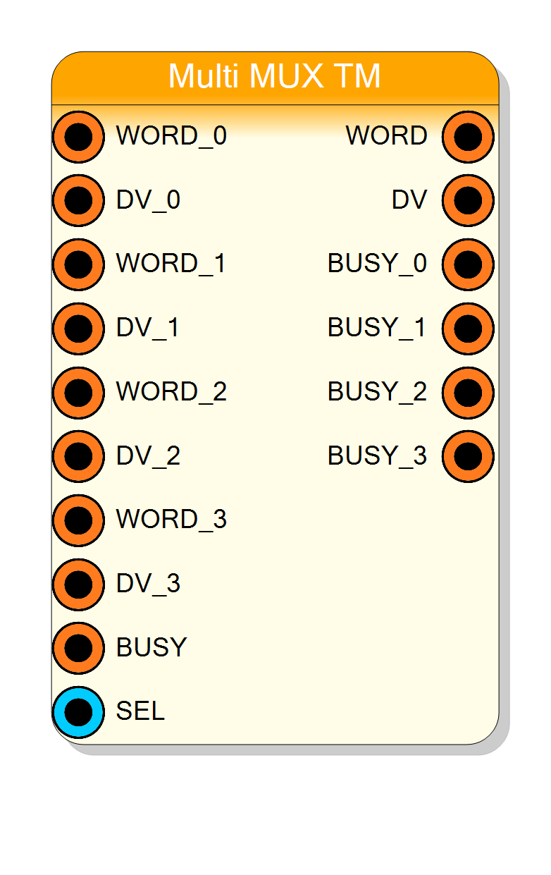
Time-multiplexed variant of the Multi MUX: multiplexes a whole SET of TM signals (data, valid, back-pressure…) with a single selector. Every data port carries
Introduction
The Multi MUX TM block is the time-multiplexed version of the Multi MUX: refer to that block’s help for the full signal-set model (forward IN->OUT signals, reverse OUT<-IN signals, per-signal Registered option, per-signal unselected value).
The only difference is the pin type: every data signal is a TM bus carrying TM factor samples per clock cycle, so a signal configured as W bits wide becomes a W x TM bit physical port. SEL is a plain vector and selects the whole channel: the routing is bus-level and identical for every sample of the TM word (there is no per-sample selection).
The TM factor (2/4/8/16/32) is chosen inside the same Multi MUX Designer window, which shows the TM row for this variant.
Pin Description
Properties
Signal set of the Multi MUX TM, produced by the Multi MUX Designer
Hidden property holding the whole signal-set configuration (including the TM factor); edit it exclusively through the Multi MUX Designer.Default: 4;4|WORD,32,F,0,0|DV,1,F,0,0|BUSY,1,R,0,1
Usage
Notes
- All the routing rules of the plain Multi MUX apply unchanged.
- The register option re-times the full TM bus at once - the latency is one clock of the fast (system) clock domain the bus lives in.
- SEL and CLK are plain 1x signals, never time-multiplexed.
Resources & Timing
-
Latency: 0 clocks (combinational signals) or 1 clock (registered signals)
-
Throughput: combinational routing, no stall
Pure LUT routing plus one register layer per registered signal. Resource usage scales with the total signal width times N times TM.