
DSP - ACCUMULATOR
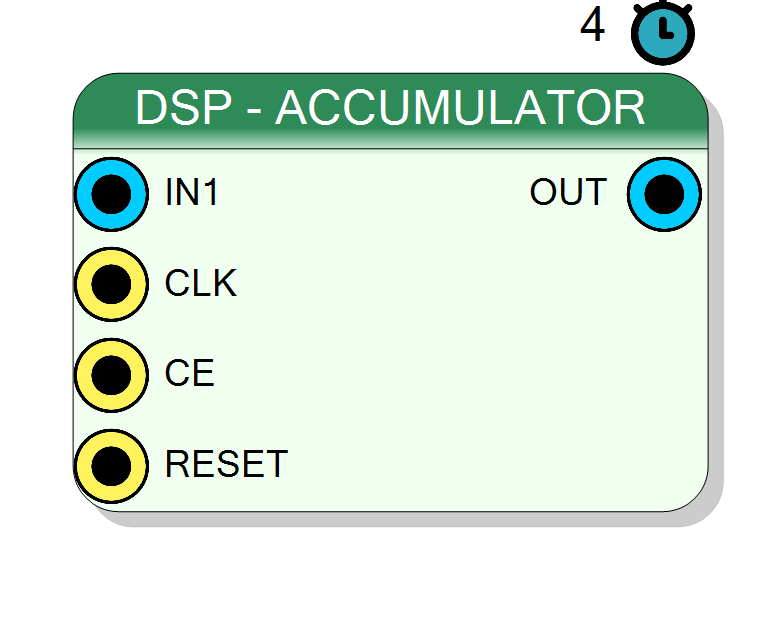
Fully-parameterizable synchronous accumulator built on top of the Xilinx primitive. It supports signed or unsigned integer streams up to 256 bit, programmable output width, and 1/2/4/8-stage pipelining for high-speed DSP designs.
Introduction
The block adds each incoming sample to an internal register, producing the
running sum on its output.
On every rising edge of CLK, if CE = 1, the accumulator performs
$$ \mathrm{OUT}(n) ;=; \mathrm{OUT}(n-1) + \mathrm{IN1}(n), $$
where the arithmetic is signed or unsigned according to the
Input sign 1 property.
A synchronous active-high RESET clears the accumulator to zero.
The internal datapath is implemented with the Xilinx c_accum IP core; the
Latency property lets you trade off clock frequency versus latency by
inserting 1, 2, 4 or 8 pipeline stages.
Pin Description
Width: Input bits 1 (2 – 256).
Arithmetic type is set by Input sign 1.
When
CE = 0 the accumulator holds its current value; pipeline registers
keep their previous state.
Forces the internal accumulator register and all pipeline stages to zero on the next rising clock edge.
Width: Accumulator Size (2 – 256).
Valid data appear after Latency clock cycles.
Properties
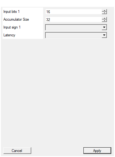
Set the number of bits of the input
Number of bits ofIN1 ($N_\text{in}$).Range 2 – 256.
Changing this value re-configures the underlying c_accum core and may update synthesis results.
Default: 16
Range: 2 – 256
Set the number of bits of the output
Width of the accumulator registerOUT ($N_\text{out}$).Range 2 – 256.
Must be ≥ Input bits 1 to avoid truncation.
Internally mapped to
C_OUT_WIDTH.
Default: 32
Range: 2 – 256
Select the sign/unsign of the input
Selects arithmetic type of IN1 and OUT:
UNSIGNED→ non-negative integers, wrap-around at $2^{N}-1$.SIGNED→ two’s-complement, range $[-2^{N-1},,2^{N-1}-1]$.
Default: UNSIGNED
Options: UNSIGNED SIGNED
Number of pipeline stages
Number of pipeline stages inserted into the accumulator datapath.Allowed values: 1, 2, 4, 8.
Directly mapped to
C_LATENCY / Latency parameters, hence
Total delay = Latency × T_CLK.Higher values increase maximum clock frequency at the cost of latency.
Default: 4
Options: 1 2 4 8
Functional description
The component realises a classic discrete–time integrator:
$$ y[n] = y[n-1] + x[n], \qquad y[-1] = 0, $$
with
x[n]→IN1y[n]→OUT
Both input and output widths are user-selectable.
If Accumulator Size > Input bits 1 the accumulator offers additional head-room,
reducing the probability of wrap-around. Arithmetic overflow follows the native
behaviour of VHDL signed/unsigned types (modulo $2^{\text{width}}$).
Mathematical background
In the $z$-domain the transfer function is
$$ H(z) = \frac{1}{1 - z^{-1}}, $$
equivalent to an ideal digital integrator. In fixed-point hardware, the effect is bounded by the chosen Accumulator Size:
$$ y_\text{max} = 2^{N_\text{out}-1}-1 \quad(\text{signed}),\qquad y_\text{max} = 2^{N_\text{out}}-1 \quad(\text{unsigned}) $$
where $N_\text{out}$ is the Accumulator Size.
Timing
The IP inserts a Latency-dependent pipeline:
| Latency property | Internal stages | Total clock cycles from IN1 to OUT |
|---|---|---|
| 1 | 1 | 1 |
| 2 | 2 | 2 |
| 4 | 4 | 4 |
| 8 | 8 | 8 |
Therefore the deterministic delay is
T_delay = Latency × T_CLK.
Typical use cases
- Digital filtering (moving–average implementation through reset control)
- Pulse-height analysis in nuclear/particle physics
- Running energy computation in SDR front-ends
- Generic DSP pipelines requiring high-speed accumulation
Waveform example
Example with pipeline delay set to 4.