
Bit-Array Synchronizer (CCCC)
Clock Crossing Chain Component for safe multi-bit synchronization between asynchronous clock domains. Implements a four-stage synchronizer chain to mitigate metastability risks when transferring data vectors across clock domains. Provides reliable Clock Domain Crossing (CDC) for control signals and status vectors up to 1024 bits wide.
Introduction
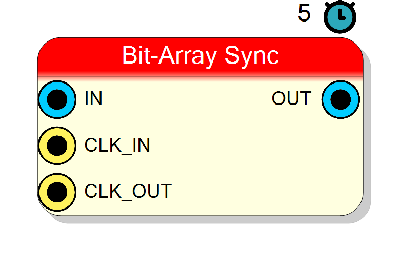
This block implements the CCCC (Clock Crossing Chain Component), a specialized synchronizer for transferring multi-bit data between asynchronous clock domains.
The CCCC operates as follows:
- Accepts data in the source clock domain (CLK_IN)
- Transfers data through a four-stage chain for metastability protection
- Outputs synchronized data in the destination clock domain (CLK_OUT)
- Processes each bit independently through identical synchronizer chains
Key characteristics:
- Four-stage synchronization: Enhanced metastability tolerance
- Multi-bit CDC: Handles vectors up to 1024 bits
- Independent bit synchronization: Each bit has its own chain
- Latency: 5 clock cycles (in destination domain)
- Critical for CDC: Essential for reliable clock domain crossing
Pin Description
Properties
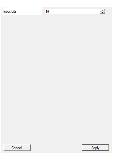
Set the number of bits of the data vector
Number of bits to synchronize (width of IN and OUT). Range: 1-1024 bits. Each bit has an independent four-stage synchronizer chain.Default: 16
Range: 1 – 1024
Functional description
The CCCC (pronounced “C-quad”) is a Clock Domain Crossing (CDC) synchronizer that safely transfers multi-bit data between asynchronous clock domains.
Synchronization chain
Each input bit passes through a four-stage flip-flop chain in the destination domain:
$$ \mathrm{OUT}[i] = \mathrm{FF}_4(\mathrm{FF}_3(\mathrm{FF}_2(\mathrm{FF}_1(\mathrm{IN}[i])))) $$
Where each $\mathrm{FF}_j$ is a flip-flop clocked by CLK_OUT.
Metastability mitigation
When signals cross clock domains, flip-flops may enter metastable states:
- Metastability: Unstable voltage level between logic ‘0’ and ‘1’
- Resolution time: Time for FF to settle to valid logic level
- MTBF: Mean Time Between Failures (metastability-induced errors)
The four-stage chain provides:
- First stage: Captures input (may go metastable)
- Stages 2-4: Allow metastability resolution
- Four stages: Very high MTBF (Mean Time Between Failures > years)
Multi-bit synchronization
WARNING: Independent bit synchronization can cause issues:
- Each bit synchronizes independently
- Bits may arrive in different clock cycles
- Multi-bit values may become corrupted during transition
This component is safe for:
- Single-bit signals
- Multi-bit signals that change infrequently
- Gray-coded counters (only one bit changes at a time)
- One-hot encoded states
- Quasi-static control signals
This component is NOT safe for:
- Binary counters (multiple bits change simultaneously)
- Data buses with arbitrary values
- High-speed data transfers
For arbitrary multi-bit data, use proper CDC techniques (handshaking, FIFOs, etc.).
Clock requirements
- CLK_IN: Source domain clock (data arrives in this domain)
- CLK_OUT: Destination domain clock (data is synchronized to this domain)
- Clocks are asynchronous: No phase or frequency relationship required
- Clocks must be free-running: No clock gating in synchronizer
Timing
| Property | Latency (CLK_OUT cycles) |
|---|---|
| CCCC | 5 |
The output appears 5 clock cycles (in the destination domain) after the input changes.
Latency breakdown
- Stage 1: Register in destination domain (may be metastable)
- Stage 2: Metastability resolution
- Stage 3: Additional resolution margin
- Stage 4: Stable output register
- Total: 4 FFs + 1 cycle = 5 clock cycle latency
Clock Domain Crossing best practices
- Single-bit signals: Prefer single-bit synchronizers for control
- Gray code: Use Gray code for multi-bit counters
- Quasi-static: Only sync slowly-changing multi-bit signals
- Handshaking: Use req/ack protocols for data transfers
- FIFOs: Use async FIFOs for high-bandwidth CDC
- No combinational logic: Never add logic between clock domains
Metastability theory
Metastability probability decreases exponentially with resolution time:
$$ MTBF = \frac{e^{t_r / \tau}}{f_{CLK} \cdot f_{DATA} \cdot T_0} $$
Where:
- $t_r$ = resolution time (more FF stages → higher $t_r$)
- $\tau$ = FF time constant
- $T_0$ = metastability window
- More stages → exponentially better MTBF
Four stages provide MTBF > 10^15 years for typical designs.
Typical use cases
- Control signal synchronization: Enable, reset, mode signals
- Status synchronization: Flags, state indicators
- Gray-coded counters: CDC for read/write pointers
- Configuration registers: Slowly-changing settings
- Interrupt signals: Async interrupt synchronization
- GPIO synchronization: External signal inputs
- Power domain crossing: Signals between power domains
Waveform example
Example showing CDC with 5-cycle latency:
Note: IN changes in source domain, OUT changes 5 cycles later in dest domain.