
A395A - LVDS/ECL Input Expansion
32-channel LVDS/ECL/PECL input expansion board for V2495. Receives external differential signals and makes them available to the FPGA logic.
Introduction
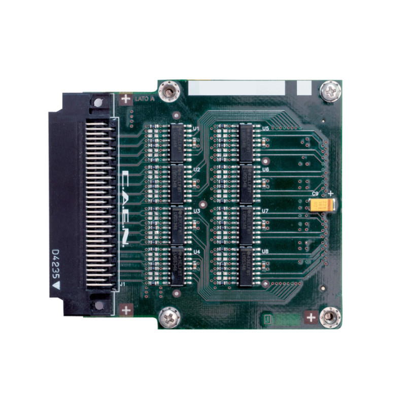
The A395A is an expansion board for the V2495 that provides 32 LVDS/ECL/PECL input channels. It can be installed in expansion slots D, E, or F of the V2495 mainboard.
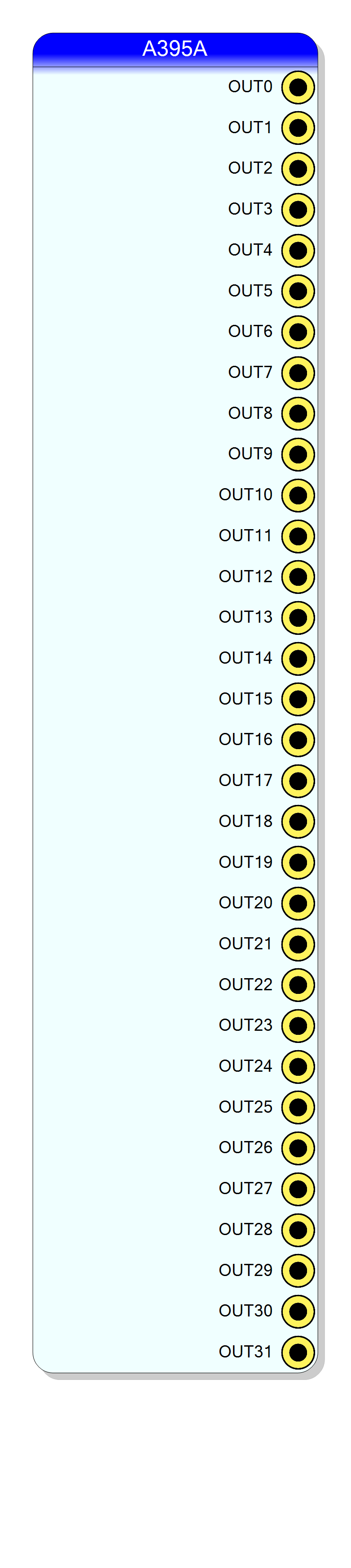
From the FPGA perspective, this board receives external signals. The 32 channels appear as outputs from the block (providing data to your logic design).
Product link: CAEN A395A
Pin Description
Output signals to FPGA logic (32 total). Each channel is a 1-bit signal representing the received external input.
These pins provide the received LVDS/ECL/PECL signals to your design.
Properties
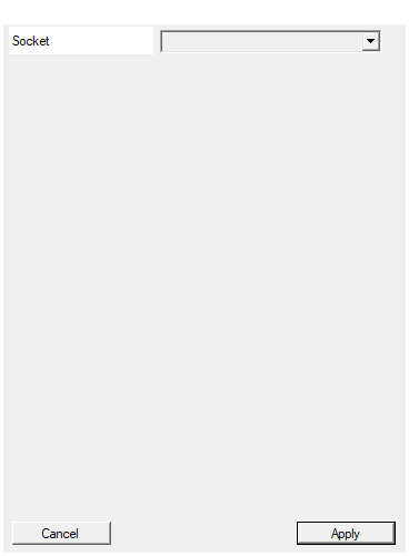
Select the socket hosting the expansion board
Selects the expansion socket where the A395A is installed. Available options: D, E, F. Must match the physical installation location on the V2495 mainboard.Default: D
Options: D E F
Usage
Signal Direction
The A395A is an input expansion - it receives signals from external equipment via LVDS/ECL/PECL differential pairs. From the SciCompiler perspective:
┌──────────────────────────────────────────────────────────────────┐
│ A395A Signal Flow │
│ │
│ External │
│ Equipment ┌─────────────┐ ┌─────────────┐ │
│ │ │ │ FPGA │ │
│ LVDS/ECL ═══►│ A395A │═══► OUT0-OUT31 ═►│ Logic │ │
│ Signals │ (32 ch) │ │ │ │
│ │ │ │ │ │
│ └─────────────┘ └─────────────┘ │
└──────────────────────────────────────────────────────────────────┘
Expansion Socket Selection
The A395A can be installed in one of three expansion sockets:
| Socket | Description |
|---|---|
| D | Expansion slot D |
| E | Expansion slot E |
| F | Expansion slot F |
Select the appropriate socket during block creation to match the physical installation.
Signal Characteristics
| Parameter | Value |
|---|---|
| Channels | 32 |
| Signal type | LVDS / ECL / PECL (differential) |
| Direction | Input to V2495 |
| Logic levels | Per LVDS/ECL/PECL specifications |
Typical Usage
Connect external differential signal sources to the A395A front panel connectors. The signals are then available inside your FPGA design via the OUT0-OUT31 pins:
External detectors/electronics ──► A395A ──► FPGA trigger logic
Resources & Timing
-
Latency: Minimal (input buffer delay only)
-
Throughput: 32 channels at FPGA clock rate
- Supports LVDS, ECL, and PECL differential signal standards
- Each channel is independently routed to FPGA
- No programmable configuration required
Supported Boards
- V2495