
NCO (Numerically Controlled Oscillator)
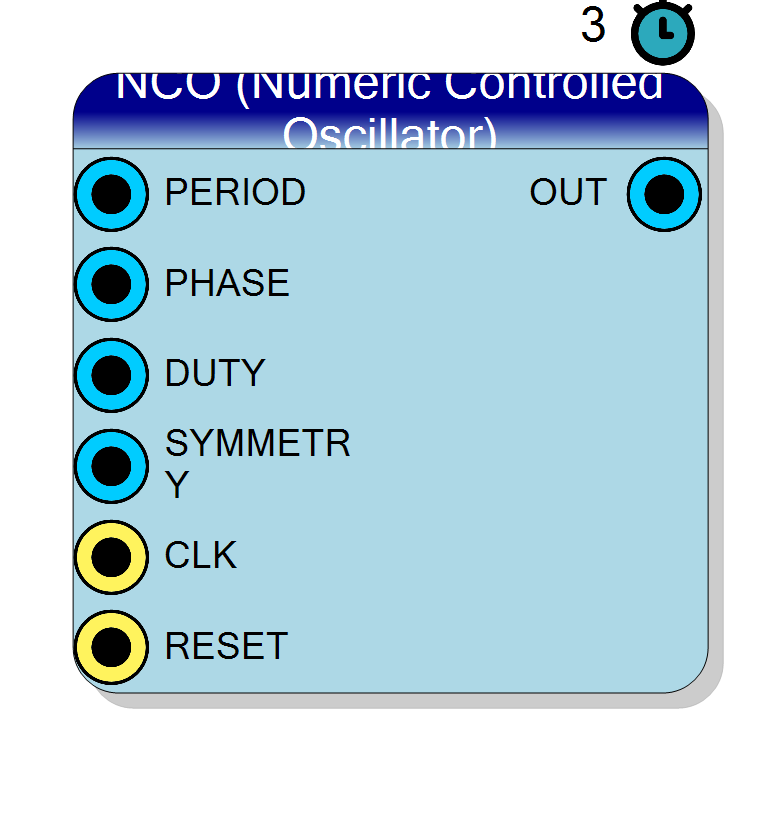
High-precision waveform generator using phase accumulator technique. Supports sine, cosine, ramp, triangle, square, and sawtooth waveforms.
Introduction
The NCO (Numerically Controlled Oscillator) block generates high-precision periodic waveforms using the phase accumulator technique. This is a fundamental building block for Direct Digital Synthesis (DDS) applications.
The NCO supports multiple waveform types (sine, cosine, ramp, triangle, square, sawtooth) with configurable output resolution, frequency precision, and phase offset.
Pin Description
Phase offset (unsigned 16-bit). Adds a constant phase shift to the output waveform.
- 0x0000 = 0°
- 0x4000 = 90°
- 0x8000 = 180°
- 0xC000 = 270°
Duty cycle control (unsigned 16-bit). Used for TRIANGLE and SQUARE waveforms.
- 0x0000 = defaults to 50%
- 0x8000 = 50%
- 0xFFFF = ~100%
Properties
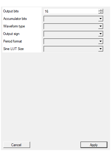
Number of bits of the output signal
Number of bits of the output signal. Range: 8 to 32, default 16.Default: 16
Range: 8 – 32
Number of bits of the internal phase accumulator (higher = better frequency resolution)
Number of bits of the internal phase accumulator. Higher values provide better frequency resolution. Available values: 32, 40, 48, 56, 64, default 48.Default: 48
Options: 32 40 48 56 64
Select the type of waveform to generate
Type of waveform to generate. Available values: SINE, COSINE, RAMP, TRIANGLE, SQUARE, SAWTOOTH, default SINE.Default: SINE
Options: SINE COSINE RAMP TRIANGLE SQUARE SAWTOOTH
Select signed or unsigned output
Output signal format. Available values: UNSIGNED, SIGNED, default SIGNED.Default: SIGNED
Options: UNSIGNED SIGNED
Select the format of the PERIOD input signal
Format of the PERIOD input signal. Available values: UINT32, FIXED16.16, FIXED24.8, FIXED40.24, default UINT32.Default: UINT32
Options: UINT32 FIXED16.16 FIXED24.8 FIXED40.24
Sine/Cosine lookup table size (larger = better resolution but more BRAM)
Sine/Cosine lookup table size. Larger values provide better waveform quality but use more BRAM. Available values: 256 (1.41° res), 512 (0.70° res), 1024 (0.35° res), 2048 (0.18° res), 4096 (0.09° res), 8192 (0.04° res), default 1024 (0.35° res).Default: 1024 (0.35° res)
Options: 256 (1.41° res) 512 (0.70° res) 1024 (0.35° res) 2048 (0.18° res) 4096 (0.09° res) 8192 (0.04° res)
Usage
Phase Accumulator Principle
The NCO uses a phase accumulator to generate periodic waveforms. The phase accumulator is an N-bit register that increments by a fixed amount (phase increment) on each clock cycle:
$$ \phi[n] = \phi[n-1] + \Delta\phi \mod 2^N $$
where:
- $\phi[n]$ is the current phase
- $\Delta\phi$ is the phase increment
- $N$ is the accumulator bit width
The phase accumulator naturally wraps around, producing a sawtooth-like phase ramp that drives the waveform generation.
Frequency Control
The output frequency is determined by the PERIOD input and the clock frequency:
$$ f_{out} = \frac{f_{clk}}{\text{PERIOD}} $$
The phase increment is calculated internally as:
$$ \Delta\phi = \frac{2^N}{\text{PERIOD}} $$
where $N$ is the accumulator bit width (32-64 bits).
Frequency Resolution
The minimum frequency step (frequency resolution) depends on the accumulator size:
$$ \Delta f = \frac{f_{clk}}{2^N} $$
| Accumulator Bits | Resolution @ 100 MHz |
|---|---|
| 32 | 0.023 Hz |
| 40 | 90.9 µHz |
| 48 | 0.355 µHz |
| 56 | 1.39 nHz |
| 64 | 5.42 pHz |
Period Format
The PERIOD input supports multiple fixed-point formats for different use cases:
| Format | Total Bits | Description |
|---|---|---|
| UINT32 | 32 | Integer period in clock cycles |
| FIXED16.16 | 32 | 16-bit integer + 16-bit fractional |
| FIXED24.8 | 32 | 24-bit integer + 8-bit fractional |
| FIXED40.24 | 64 | 40-bit integer + 24-bit fractional |
Fractional formats allow sub-sample frequency control for higher precision.
Waveform Types
The NCO can generate the following waveforms:
| Waveform | Description |
|---|---|
| SINE | Sinusoidal wave using lookup table |
| COSINE | Cosine wave (sine with 90° phase shift) |
| RAMP | Linear ramp from minimum to maximum |
| TRIANGLE | Symmetric triangular wave |
| SQUARE | Square wave with adjustable duty cycle |
| SAWTOOTH | Inverted ramp from maximum to minimum |
Sine/Cosine Generation
For SINE and COSINE waveforms, the NCO uses a lookup table (LUT) containing pre-computed sine values. The phase accumulator’s upper bits index into the LUT.
| LUT Size | Angular Resolution |
|---|---|
| 256 | 1.41° |
| 512 | 0.70° |
| 1024 | 0.35° |
| 2048 | 0.18° |
| 4096 | 0.09° |
| 8192 | 0.04° |
Larger LUTs provide better waveform quality (lower spurious content) but consume more BRAM.
Duty Cycle Control
For TRIANGLE and SQUARE waveforms, the DUTY input controls the symmetry:
- SQUARE: DUTY determines the HIGH time percentage
- TRIANGLE: DUTY determines the rising edge percentage
The DUTY input is a 16-bit unsigned value where:
- 0x0000 = 0% (falls back to 50%)
- 0x8000 = 50%
- 0xFFFF = 100%
Phase Offset
The PHASE input adds a constant phase offset to the output:
$$ \phi_{total} = \phi_{acc} + \phi_{offset} $$
The PHASE input is a 16-bit unsigned value representing the phase in the range [0, 2π):
- 0x0000 = 0°
- 0x4000 = 90°
- 0x8000 = 180°
- 0xC000 = 270°
Output Format
The output can be configured as:
- Signed: Output ranges from $-(2^{N-1})$ to $(2^{N-1}-1)$
- Unsigned: Output ranges from 0 to $(2^N-1)$
where N is the output bit width (8-32 bits).
Timing
| Parameter | Value |
|---|---|
| Pipeline Latency | 3 clock cycles |
| Throughput | 1 sample per clock cycle (II=1) |
The output is updated on every clock cycle with a fixed latency of 3 clock cycles from input to output.
Resources & Timing
-
Latency: 3 clock cycles
-
Throughput: 1 sample per clock cycle (II=1)
HLS-based implementation. Resource usage varies with LUT size and accumulator width.