
Petiroc Trigger
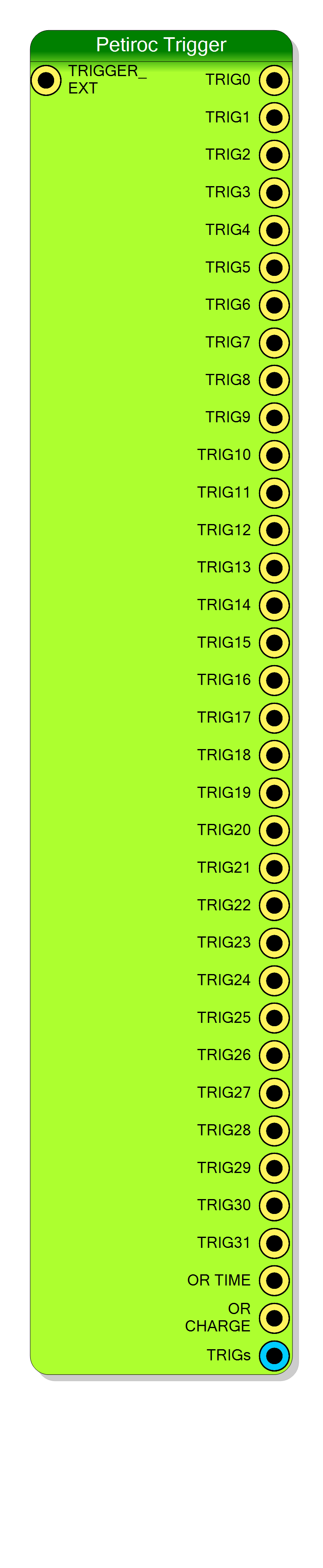
Board-pin block that exposes the fast discriminator outputs of one PETIROC-2A ASIC to the design: the 32 per-channel triggers (as individual pins and as a 32-bit bus), the two chip-level OR outputs, and the external-trigger input of the same ASIC. It contains no logic of its own - it is a named connection to the DT5550W board support wrapper.
Introduction
Principle of Operation
Each of the 32 channels of the PETIROC-2A has a fast time discriminator. The ASIC drives one trigger line per channel plus two chip-level OR outputs (time OR and charge OR). On the DT5550W those lines arrive at the FPGA and are made available to a SciCompiler design through this block.
The block generates no hardware. CompileHDL does not instantiate any
entity and writes no .vhd: it calls GenerateServiceHDL and then emits one
plain concurrent assignment per connected pin, binding the pin’s net to the
board-support signal of the selected ASIC:
-- outputs (one line per connected pin)
<net of TRIG0> <= A_TRIG0;
<net of OR_TIME> <= A_OR_TIME;
<net of OR_CHARGE> <= A_OR_CHARGE;
<net of TRIGs> <= A_TRIGs;
-- inputs
TRIGGER_EXT_A_s <= <net of TRIGGER_EXT>;
The A_ prefix is the ASIC property (A, B, C, D). Because the
block is a pure alias, it costs no logic, adds no latency and introduces no
register stage: whatever the board wrapper presents is what the pin carries,
in the same clock cycle.
Pins you leave unconnected are skipped entirely (the generator checks
UsingOpenOrDefaultConnection), so an unused trigger pin emits no assignment
and no dangling net.
Pin Description
TRIGGER_EXT_<ASIC>_s, which reaches an ASIC external-trigger pad.
Use it to force a conversion from the design (software pulse, LEMO input,
coincidence between two chips). Leave it open if the ASIC is to trigger
only on its own discriminators - an unconnected pin emits no assignment at
all and the board signal keeps its default '0'.
See the alert in the description about the crossed A↔D / B↔C mapping.
not A_TRG(0) at board level). Combinational, no
register stage. Identical to TRIGs(0).
TRIG0. Identical to TRIGs(1).
TRIG0. Identical to TRIGs(2).
TRIG0. Identical to TRIGs(3).
TRIG0. Identical to TRIGs(4).
TRIG0. Identical to TRIGs(5).
TRIG0. Identical to TRIGs(6).
TRIG0. Identical to TRIGs(7).
TRIG0. Identical to TRIGs(8).
TRIG0. Identical to TRIGs(9).
TRIG0. Identical to TRIGs(10).
TRIG0. Identical to TRIGs(11).
TRIG0. Identical to TRIGs(12).
TRIG0. Identical to TRIGs(13).
TRIG0. Identical to TRIGs(14).
TRIG0. Identical to TRIGs(15).
TRIG0. Identical to TRIGs(16).
TRIG0. Identical to TRIGs(17).
TRIG0. Identical to TRIGs(18).
TRIG0. Identical to TRIGs(19).
TRIG0. Identical to TRIGs(20).
TRIG0. Identical to TRIGs(21).
TRIG0. Identical to TRIGs(22).
TRIG0. Identical to TRIGs(23).
TRIG0. Identical to TRIGs(24).
TRIG0. Identical to TRIGs(25).
TRIG0. Identical to TRIGs(26).
TRIG0. Identical to TRIGs(27).
TRIG0. Identical to TRIGs(28).
TRIG0. Identical to TRIGs(29).
TRIG0. Identical to TRIGs(30).
TRIG0. Identical to TRIGs(31).
not and_reduce(A_TRG), i.e. an OR
over the active-low per-channel triggers; it is not a coincidence
output. This is the usual trigger source for the Petiroc Digital
block.
not OR_CHARGE_A at board level). Fires on the charge branch rather than
the time branch; typical trigger source for the Petiroc Analog block.
TRIGs(i) = TRIG<i>. Convenient for multiplicity counting, hit-pattern
histogramming or masking whole groups of channels in one expression.
Properties
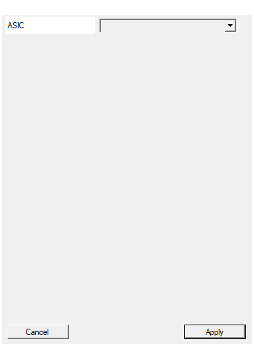
Select the ASIC to be connected to the Endpoint
Selects which of the four PETIROC-2A chips of the DT5550W this block is
bound to. The value is pasted verbatim into every emitted assignment, so
A produces A_TRIG0, A_OR_TIME, TRIGGER_EXT_A_s and so on.
| Value | Board signal prefix |
|---|---|
A |
A_* / TRIGGER_EXT_A_s |
B |
B_* / TRIGGER_EXT_B_s |
C |
C_* / TRIGGER_EXT_C_s |
D |
D_* / TRIGGER_EXT_D_s |
The property is marked isVisible = False: it is not shown in the
property grid, the board plug-in assigns it when the block is placed on a
given ASIC. Changing it does not rebuild the symbol
(RedesignIfChanged = False) because the pin list is the same for all
four chips.
Default: A
Default: A
Options: A B C D
⚙️ Detailed Operation
What the board wrapper puts on these signals
The DT5550W-PETIROC board support file (dt5550w_top.vht) builds the signals
this block reads. The ASIC’s trigger outputs are active low; the board
inverts them, so every pin of this block is active high:
| Block pin | Board signal | Board expression |
|---|---|---|
TRIG0 … TRIG31 |
A_TRIG0 … A_TRIG31 |
A_TRIGn(0) <= not A_TRG(n); |
TRIGs |
A_TRIGs |
A_TRIGs <= not A_TRG; |
OR_TIME |
A_OR_TIME |
A_OR_TIME(0) <= not and_reduce(A_TRG); |
OR_CHARGE |
A_OR_CHARGE |
A_OR_CHARGE(0) <= not OR_CHARGE_A; |
TRIGGER_EXT |
TRIGGER_EXT_A_s |
drives an ASIC *_TRIG_EXT pad |
Two consequences worth noting:
TRIGsand the 32 individualTRIG<i>pins carry exactly the same information.TRIGs(i)andTRIG<i>are driven from the sameA_TRG(i)bit. Use the bus when you want to feed a multiplicity counter or a hit pattern, the individual pins when you want to wire a single channel.OR_TIMEisnot and_reduce(A_TRG), i.e. the OR of the 32 active-low channel triggers: it is high as soon as any channel fires. It is not a coincidence/AND output.
Typical use
Petiroc Trigger rest of the design
┌───────────────┐
│ TRIG0 ───┼──► per-channel rate counter
│ … │
│ TRIG31 ───┤
│ TRIGs ───┼──► multiplicity / hit pattern
│ OR_TIME ───┼──► "Petiroc Digital" TRIG (start a readout)
│ OR_CHARGE ───┼──► "Petiroc Analog" TRIG
│ │
│ TRIGGER_EXT ◄─┼── software / LEMO / coincidence logic
└───────────────┘
OR_TIME (any channel over the time threshold) is the natural trigger source
for Petiroc Digital, which starts the ASIC conversion and reads back the
TDC/ADC frame. TRIGGER_EXT goes the other way: it lets the design force a
conversion on the ASIC independently of its internal discriminators.
One instance per ASIC
The block is bound to a single ASIC through the hidden ASIC property, which the board plug-in sets when the component is placed. Four instances (A, B, C, D) give access to all four PETIROC chips of a DT5550W. Two instances that resolve to the same ASIC letter would emit two drivers on the same board signal - place one instance per ASIC.
Failure modes
This block cannot fail at compile time: it has no generics, no resource file and no validation. The only message it prints is the informational
Generating HDL code For <designator>
If a pin appears dead, the cause is upstream of the block (the ASIC’s discriminators are configured through Petiroc Slow Control - trigger thresholds, per-channel masks and the 10-bit DACs all live in the 640-bit configuration bitstream).