
RAM Single Port
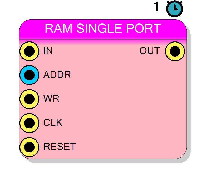
Single-port Random Access Memory with configurable depth and width. Provides read and write operations through a shared address port. Data is written when WR=1 and read otherwise. Features 1 clock cycle read latency. Uses FPGA block RAM for efficient storage.
Introduction
This block implements a single-port RAM where read and write operations share the same address port. Write operations occur when WR=1; read operations occur when WR=0.
Read latency: 1 clock cycle (registered output).
Pin Description
Properties
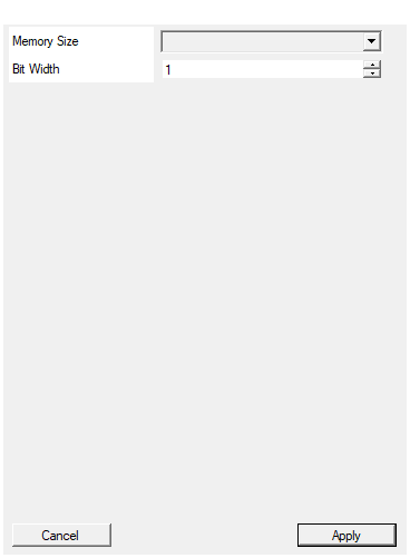
Set the amount of memory in number of words
Number of words in RAM. Allowed: 64-65536. Determines address range.Default: 1024
Options: 64 128 256 512 1024 2048 4096 8192 16384 32756 65536
Set the size in bits of the data
Bit width per word. Range: 1-1024. Total RAM = MemorySize × BusWidth bits.Default: 1
Range: 1 – 1024
Functional description
Single-port RAM uses one address port for both read and write:
- When WR=1: Writes IN data to address ADDR
- When WR=0: Reads data from address ADDR to OUT (1 cycle later)
Cannot read and write simultaneously to different addresses.
Timing
Write: Data written on rising edge when WR=1. Read: Data available 1 cycle after ADDR provided with WR=0.
Typical use cases
- Simple data storage
- Lookup tables
- Small buffers