
FIFO (Altera/Intel)
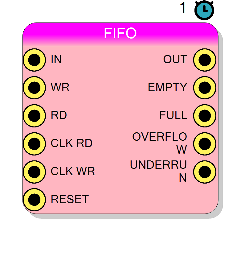
First-In-First-Out queue optimized for Intel (Altera) FPGAs. Functionally identical to FIFO_XLX but uses Intel FPGA primitives. Features independent read/write clocks, programmable thresholds, and status flags.
Introduction
This block implements a FIFO buffer using Intel (Altera) FPGA primitives. Functionally equivalent to the Xilinx FIFO but optimized for Intel architecture.
See the main FIFO documentation for detailed operation.
Pin Description
Properties
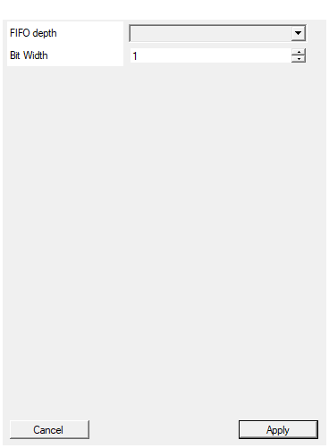
Set the amount of memory in number of words
FIFO depth. Allowed: 64-65536.Default: 1024
Options: 64 128 256 512 1024 2048 4096 8192 16384 32756 65536
Set the size in bits of the data
Bit width per word. Range: 1-1024.Default: 1
Range: 1 – 1024
Functional description
Identical to FIFO_XLX but uses Intel/Altera megafunctions for implementation. Refer to the standard FIFO component documentation for detailed behavior.