
Single Clock Delay [TM]
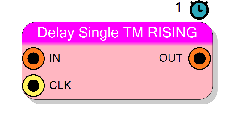
Time-multiplexed single-cycle register delay. Delays each TM phase by exactly one clock cycle with configurable edge sensitivity. All phases delayed independently in parallel. Synchronous reset, 1 clock cycle latency. TM factors: 2-32, bit widths: 1-2048.
Introduction
This block implements a time-multiplexed version of the single-cycle delay register. Each TM phase is delayed independently by exactly one clock cycle.
For each phase $i$ of the TM stream:
$$ \mathrm{OUT}_i(n) = \mathrm{IN}_i(n-1), $$
where $n$ represents the current clock cycle. All phases share the same clock and reset signals but maintain independent data paths.
Pin Description
Input bits × TM Factor
Each TM phase occupies Input bits of the bus.
Input bits × TM Factor
Each phase delayed by 1 clock cycle independently.
Properties
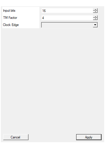
Set the number of bits of the input (per phase)
Number of bits per TM phase. Range: 1 – 2048. Total register width = InputSize × TMFactor.Default: 16
Range: 1 – 2048
Time Multiplexing factor (number of phases)
Time-multiplexing factor (number of parallel phases). Range: 2 – 32. Each phase delayed independently.Default: 4
Range: 2 – 32
Select between rising and falling edge
Clock edge sensitivity (applies to all phases). RISING: update on rising edge. FALLING: update on falling edge. Default: RISING.Default: RISING
Options: RISING FALLING
Functional description
The component implements N independent registers (where N = TM Factor), one for each TM phase. All registers operate synchronously on the same clock but process different data slices.
TM operation
The input bus is partitioned into N slices, one per phase:
- Phase 0: bits [InputSize-1 : 0]
- Phase 1: bits [2×InputSize-1 : InputSize]
- Phase i: bits [(i+1)×InputSize-1 : i×InputSize]
Each slice is independently delayed by 1 clock cycle.
Implementation note
The TM version reuses the same sc_delay.vhd entity but with IN_SIZE set to
InputSize × TMFactor. This creates a wide register that delays the entire
TM bus in parallel.
Timing diagram
Example with TM Factor = 4, Input Size = 8 bits per phase:
Note: All 4 phases delayed in parallel by 1 clock cycle.
Mathematical background
In TM systems, the delay operator applies independently to each phase:
$$ Y_i(z) = z^{-1} \cdot X_i(z), \quad \forall i \in [0, N-1] $$
where $N$ is the TM Factor. Each phase maintains its own delay line but shares the same clock.
Timing
Fixed latency: 1 clock cycle (same as non-TM version)
| Property | Latency (clock cycles) |
|---|---|
| Single Clock Delay TM | 1 |
All TM phases have identical, deterministic latency.
Typical use cases
- TM pipeline stages: Inserting registers in TM datapaths
- Delay matching: Aligning TM signals with different processing delays
- Multi-channel synchronization: Buffering parallel detector channels
- Timing closure: Breaking long paths in TM designs
- Phase alignment: Compensating for skew in TM processing chains
Design considerations
- Resource usage: Total flip-flops = InputSize × TMFactor
- Bus width: Total input/output width = InputSize × TMFactor (can be large!)
- Reset behavior: All phases reset to zero simultaneously
- Independent phases: Each phase delayed separately, no inter-phase coupling