
Citiroc Trigger - V2
Access point to the 32 channel discriminator outputs of one CITIROC 1A ASIC on the DT5550W-Citiroc1A-V2 board, with a 32-bit channel mask applied in the FPGA, the two chip-level OR outputs, the two chip-level NOR outputs and the external trigger input of the chip. The block contains no logic: it connects board wrapper signals to your nets.

Introduction
Principle of Operation
Each CITIROC 1A channel has a fast discriminator whose output leaves the chip on its own pin. On the DT5550W-Citiroc1A-V2 the 32 outputs of every ASIC arrive at the FPGA as a 32-bit input bus, and the board wrapper puts a channel mask in front of them before anything else sees them:
TRIGn <= A_TRG(n) and (not MASK(n)) -- per channel
TRIGs <= A_TRG and (not MASK) -- as a vector
OR_TIME <= or_reduce(TRIGs) -- OR of the surviving channels
A mask bit set to '1' therefore disables that channel, and because OR_TIME is
computed after the mask, masking a noisy channel also removes it from the global time
trigger. This is the main functional difference with the first-generation Citiroc
Trigger block, where the mask does not exist and OR_TIME comes from a chip pin.
The block itself instantiates nothing: CompileHDL emits only concurrent assignments
<your net> <= A_TRIG0; -- for every connected output
TRIGGER_MASK_A <= <your net>; -- for MASK
TRIGGER_EXT_A_s <= <your net>; -- for TRIGGER_EXT
so there is no clock, no reset, no latency and no resource cost beyond the 32 AND gates the board wrapper already contains.
Pin Description
TRIG_EXT input pin. Left unconnected, no HDL is emitted and the board signal
stays at '0'.
'1' forces channel
n to '0' on TRIGn, on bit n of TRIGs and inside OR_TIME. Purely
combinational - the mask takes effect in the same cycle it changes.
Left unconnected, no assignment is emitted and the board default X"00000000" applies,
i.e. all 32 channels enabled.
The mask is applied in the FPGA only: the chip’s own OR_CHARGE, NOR_TIME and
NOR_CHARGE outputs and the analog readout are not affected by it.
TRIG0 = A_TRG(0) and not MASK(0). High while the channel’s trigger
output is asserted and bit 0 of MASK is '0'.
Asynchronous to the design clock - resynchronise before use.
An unconnected output emits no HDL at all.
TRIG1 = A_TRG(1) and not MASK(1). High while the channel’s trigger
output is asserted and bit 1 of MASK is '0'.
Asynchronous to the design clock - resynchronise before use.
An unconnected output emits no HDL at all.
TRIG2 = A_TRG(2) and not MASK(2). High while the channel’s trigger
output is asserted and bit 2 of MASK is '0'.
Asynchronous to the design clock - resynchronise before use.
An unconnected output emits no HDL at all.
TRIG3 = A_TRG(3) and not MASK(3). High while the channel’s trigger
output is asserted and bit 3 of MASK is '0'.
Asynchronous to the design clock - resynchronise before use.
An unconnected output emits no HDL at all.
TRIG4 = A_TRG(4) and not MASK(4). High while the channel’s trigger
output is asserted and bit 4 of MASK is '0'.
Asynchronous to the design clock - resynchronise before use.
An unconnected output emits no HDL at all.
TRIG5 = A_TRG(5) and not MASK(5). High while the channel’s trigger
output is asserted and bit 5 of MASK is '0'.
Asynchronous to the design clock - resynchronise before use.
An unconnected output emits no HDL at all.
TRIG6 = A_TRG(6) and not MASK(6). High while the channel’s trigger
output is asserted and bit 6 of MASK is '0'.
Asynchronous to the design clock - resynchronise before use.
An unconnected output emits no HDL at all.
TRIG7 = A_TRG(7) and not MASK(7). High while the channel’s trigger
output is asserted and bit 7 of MASK is '0'.
Asynchronous to the design clock - resynchronise before use.
An unconnected output emits no HDL at all.
TRIG8 = A_TRG(8) and not MASK(8). High while the channel’s trigger
output is asserted and bit 8 of MASK is '0'.
Asynchronous to the design clock - resynchronise before use.
An unconnected output emits no HDL at all.
TRIG9 = A_TRG(9) and not MASK(9). High while the channel’s trigger
output is asserted and bit 9 of MASK is '0'.
Asynchronous to the design clock - resynchronise before use.
An unconnected output emits no HDL at all.
TRIG10 = A_TRG(10) and not MASK(10). High while the channel’s trigger
output is asserted and bit 10 of MASK is '0'.
Asynchronous to the design clock - resynchronise before use.
An unconnected output emits no HDL at all.
TRIG11 = A_TRG(11) and not MASK(11). High while the channel’s trigger
output is asserted and bit 11 of MASK is '0'.
Asynchronous to the design clock - resynchronise before use.
An unconnected output emits no HDL at all.
TRIG12 = A_TRG(12) and not MASK(12). High while the channel’s trigger
output is asserted and bit 12 of MASK is '0'.
Asynchronous to the design clock - resynchronise before use.
An unconnected output emits no HDL at all.
TRIG13 = A_TRG(13) and not MASK(13). High while the channel’s trigger
output is asserted and bit 13 of MASK is '0'.
Asynchronous to the design clock - resynchronise before use.
An unconnected output emits no HDL at all.
TRIG14 = A_TRG(14) and not MASK(14). High while the channel’s trigger
output is asserted and bit 14 of MASK is '0'.
Asynchronous to the design clock - resynchronise before use.
An unconnected output emits no HDL at all.
TRIG15 = A_TRG(15) and not MASK(15). High while the channel’s trigger
output is asserted and bit 15 of MASK is '0'.
Asynchronous to the design clock - resynchronise before use.
An unconnected output emits no HDL at all.
TRIG16 = A_TRG(16) and not MASK(16). High while the channel’s trigger
output is asserted and bit 16 of MASK is '0'.
Asynchronous to the design clock - resynchronise before use.
An unconnected output emits no HDL at all.
TRIG17 = A_TRG(17) and not MASK(17). High while the channel’s trigger
output is asserted and bit 17 of MASK is '0'.
Asynchronous to the design clock - resynchronise before use.
An unconnected output emits no HDL at all.
TRIG18 = A_TRG(18) and not MASK(18). High while the channel’s trigger
output is asserted and bit 18 of MASK is '0'.
Asynchronous to the design clock - resynchronise before use.
An unconnected output emits no HDL at all.
TRIG19 = A_TRG(19) and not MASK(19). High while the channel’s trigger
output is asserted and bit 19 of MASK is '0'.
Asynchronous to the design clock - resynchronise before use.
An unconnected output emits no HDL at all.
TRIG20 = A_TRG(20) and not MASK(20). High while the channel’s trigger
output is asserted and bit 20 of MASK is '0'.
Asynchronous to the design clock - resynchronise before use.
An unconnected output emits no HDL at all.
TRIG21 = A_TRG(21) and not MASK(21). High while the channel’s trigger
output is asserted and bit 21 of MASK is '0'.
Asynchronous to the design clock - resynchronise before use.
An unconnected output emits no HDL at all.
TRIG22 = A_TRG(22) and not MASK(22). High while the channel’s trigger
output is asserted and bit 22 of MASK is '0'.
Asynchronous to the design clock - resynchronise before use.
An unconnected output emits no HDL at all.
TRIG23 = A_TRG(23) and not MASK(23). High while the channel’s trigger
output is asserted and bit 23 of MASK is '0'.
Asynchronous to the design clock - resynchronise before use.
An unconnected output emits no HDL at all.
TRIG24 = A_TRG(24) and not MASK(24). High while the channel’s trigger
output is asserted and bit 24 of MASK is '0'.
Asynchronous to the design clock - resynchronise before use.
An unconnected output emits no HDL at all.
TRIG25 = A_TRG(25) and not MASK(25). High while the channel’s trigger
output is asserted and bit 25 of MASK is '0'.
Asynchronous to the design clock - resynchronise before use.
An unconnected output emits no HDL at all.
TRIG26 = A_TRG(26) and not MASK(26). High while the channel’s trigger
output is asserted and bit 26 of MASK is '0'.
Asynchronous to the design clock - resynchronise before use.
An unconnected output emits no HDL at all.
TRIG27 = A_TRG(27) and not MASK(27). High while the channel’s trigger
output is asserted and bit 27 of MASK is '0'.
Asynchronous to the design clock - resynchronise before use.
An unconnected output emits no HDL at all.
TRIG28 = A_TRG(28) and not MASK(28). High while the channel’s trigger
output is asserted and bit 28 of MASK is '0'.
Asynchronous to the design clock - resynchronise before use.
An unconnected output emits no HDL at all.
TRIG29 = A_TRG(29) and not MASK(29). High while the channel’s trigger
output is asserted and bit 29 of MASK is '0'.
Asynchronous to the design clock - resynchronise before use.
An unconnected output emits no HDL at all.
TRIG30 = A_TRG(30) and not MASK(30). High while the channel’s trigger
output is asserted and bit 30 of MASK is '0'.
Asynchronous to the design clock - resynchronise before use.
An unconnected output emits no HDL at all.
TRIG31 = A_TRG(31) and not MASK(31). High while the channel’s trigger
output is asserted and bit 31 of MASK is '0'.
Asynchronous to the design clock - resynchronise before use.
An unconnected output emits no HDL at all.
or_reduce(A_TRG and not MASK)). High while at least one unmasked channel fires.
This is the pin to use as the event trigger, because it honours MASK.
Asynchronous to the design clock, and as narrow as the discriminator pulse itself -
shape it with a Monostable before using it.
OR32 charge output pin, passed straight through
(A_OR_CHARGE(0) <= A_OR32). Produced inside the chip, therefore not affected by
MASK.
Asynchronous to the design clock.
NOR32 time output pin as it comes, with no
inversion and no masking (A_NOR_T(0) <= A_NOR_TIME). Being a NOR it is the
complement of the chip’s internal time OR.
Asynchronous to the design clock.
NOR32 charge output pin as it comes, with no
inversion and no masking (A_NOR_C(0) <= A_NOR_CHARGE).
Asynchronous to the design clock.
A_TRIGs <= A_TRG and not TRIGGER_MASK_A). Use it as the hit pattern to latch
together with a readout frame.
Asynchronous to the design clock - latch it with the trigger that started the event.
Properties
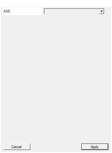
Select the ASIC to be connected to the Endpoint
Which of the four CITIROC sites on the board this block is wired to. It selects the prefix used in the generated assignments (A_TRIG0 / TRIGGER_MASK_A,
B_TRIG0 / TRIGGER_MASK_B, …), so to read the triggers of several ASICs you place
one block per chip.
Valid values: A, B, C, D.
Default: A.
Default: A
Options: A B C D
Detailed Operation
What each pin really is, on this board
Taken from the DT5550W-Citiroc1A-V2 board wrapper (dt5550w_top.vht):
| Symbol pin | Board wrapper expression | Origin |
|---|---|---|
TRIG0..TRIG31 |
A_TRIGn(0) <= A_TRG(n) and (not TRIGGER_MASK_A(n)) |
discriminator pin n, masked |
TRIGs |
A_TRIGs <= A_TRG and (not TRIGGER_MASK_A) |
the 32 masked bits as one vector |
OR_TIME |
A_OR_TIME(0) <= or_reduce(A_TRIGs) |
computed in the FPGA from the masked triggers |
OR_CHARGE |
A_OR_CHARGE(0) <= A_OR32 |
the chip’s OR32 charge output pin |
NOR_TIME |
A_NOR_T(0) <= A_NOR_TIME |
the chip’s NOR32 time output pin, not inverted |
NOR_CHARGE |
A_NOR_C(0) <= A_NOR_CHARGE |
the chip’s NOR32 charge output pin |
MASK |
TRIGGER_MASK_A <= <your net> |
FPGA-side mask, '1' disables a channel |
TRIGGER_EXT |
A_TRIG_EXT <= TRIGGER_EXT_A_s(0) |
an FPGA output pin driving the chip’s external trigger input |
So this block gives you the OR outputs and the NOR outputs of the chip at the same
time. OR_TIME is the only one of the four that is not a chip pin: it is the OR of the
masked channel triggers, so it follows the mask while NOR_TIME, OR_CHARGE and
NOR_CHARGE do not.
The mask
MASK is a plain 32-bit combinational input - there is no register, no write strobe and
no clock. Drive it from a Register File output, from constants, or from your own logic;
the effect is immediate.
MASK(n) = '0'- channel n passes toTRIGn, to bit n ofTRIGs, and contributes toOR_TIME.MASK(n) = '1'- channel n is forced to'0'everywhere, including inOR_TIME.MASKleft unconnected - no assignment is emitted and the board signal keeps its declared defaultX"00000000", i.e. all channels enabled.
Masking here is an FPGA-side gate. It silences a channel for the FPGA logic only; the
chip still discriminates it, so a masked channel still appears in the chip’s own
OR_CHARGE / NOR_TIME / NOR_CHARGE outputs and still takes part in the analog
readout.
Emitted HDL
One concurrent assignment per connected pin; unconnected pins emit nothing at all, so
an unused TRIGs or an unused MASK costs nothing and leaves the board default in place.
Typical use
- Noisy-channel suppression - a 32-bit register from the host into
MASKlets the operator disable channels at run time without rebuilding the firmware, and the globalOR_TIMEtrigger follows immediately. - Event trigger -
OR_TIMEinto a Monostable to produce the single-cycle strobe that starts the Citiroc Analog - V2 readout. - Hit pattern -
TRIGslatched with the event. - Chip-level comparison -
NOR_TIME/NOR_CHARGEnext toOR_TIMEto compare what the chip sees with what survives the mask.
Differences with the first-generation Citiroc Trigger
| Citiroc Trigger | Citiroc Trigger - V2 (this block) | |
|---|---|---|
| Board | DT5550W-Citiroc1A | DT5550W-Citiroc1A-V2 |
| Pins | 36 | 39 |
| Extra pins | - | NOR_TIME, NOR_CHARGE, MASK |
TRIGn / TRIGs |
raw A_TRG |
A_TRG and not MASK |
OR_TIME |
not A_NOR_TIME (chip pin, inverted) |
or_reduce(TRIGs), computed in the FPGA after the mask |
OR_CHARGE |
A_OR32 |
A_OR32 (identical) |
TRIGGER_EXT pad type |
std_logic, emitted as TRIGGER_EXT_A_s <= <net>(0); |
std_logic_vector, emitted as TRIGGER_EXT_A_s <= <net>; |
The ASIC property, the absence of clock/reset/logic and the version string 1.1.0.0
are the same in both.
Resources & Timing
-
Latency: None - the block emits concurrent assignments only, no register and no clock
-
Throughput: Not applicable
- No VHDL file is written to
pcores/and no logic is inferred by the block itself; the 32 AND gates of the mask live in the board wrapper. - Only available on the DT5550W-Citiroc1A-V2 board (board GUID
26E86B08-6FEF-4B0F-8872-793CC478DA97). - Not available inside a subpage and not available in a state machine.