
HV Controller
I2C-based High Voltage controller interface for the DT5550W board. Provides communication with the A7585D HV power supply module.
Introduction
The HV Controller block provides an I2C interface for controlling the A7585D High Voltage power supply module on the DT5550W board. This specialized component handles all the low-level I2C communication required for HV control and monitoring.
The A7585D is a compact, high-performance HV module used in detector applications:
- Output voltage range: 0 to 80V (adjustable)
- Communication: I2C interface
- Features: Voltage/current readback, temperature monitoring, overcurrent protection
This component operates similarly to the I2C Master but is pre-configured for the HV Controller interface.
Pin Description
Properties
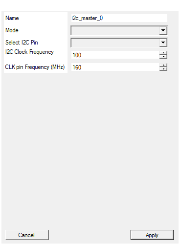
Set the name of the endpoint
Default: i2c_master_0
Select between memory mapped petipheral and FPGA control mode. In memory mapped mode the core can be controlled only via register from PC
Default: Memory Mapped
Options: FPGA Memory Mapped
Select the I2C pin to be used by the code.
Default: IIC
Options: IIC
Set SCL frequency for the I2C master
Default: 100
Range: 1 – 400
Set the pin clock frequency in order to correcly calculate the scaler frequency
Default: 160
Range: 1 – 500
Operation mode selection.
- Memory Mapped: PC software controls HV via SDK
- FPGA: FPGA logic controls HV with exposed pins Default: Memory Mapped.
I2C clock frequency in KHz for A7585D communication.
- Range: 1 to 400 KHz
- Default: 100 KHz Note: A7585D supports up to 400 KHz (I2C Fast Mode).
Input clock frequency driving the I2C controller.
- Range: 1 to 500 MHz
- Default: 160 MHz Must match the actual clock connected to the component.
Usage
When to Use HV Controller
Use this component when you need to:
- Control HV output: Set output voltage level for detectors
- Monitor HV status: Read actual voltage, current, and temperature
- Manage protection: Handle overcurrent and overtemperature conditions
- Integrate HV control: Include HV management in your FPGA design
Operation Modes
Like the I2C Master, the HV Controller supports two modes:
| Mode | Description | Use Case |
|---|---|---|
| Memory Mapped | Software-controlled via SDK | Simple HV control from PC |
| FPGA | FPGA logic controlled with pins | Automated HV management |
A7585D Communication
The A7585D uses a register-based I2C protocol:
┌─────────────────────────────────────────┐
│ A7585D Registers │
├─────────────────────────────────────────┤
│ Address │ Register │ Access │
├─────────┼────────────────┼─────────────┤
│ 0x00 │ Control │ Read/Write │
│ 0x01 │ Status │ Read │
│ 0x02 │ Voltage Set │ Read/Write │
│ 0x03 │ Voltage Read │ Read │
│ 0x04 │ Current Read │ Read │
│ 0x05 │ Temperature │ Read │
└─────────┴────────────────┴─────────────┘
Typical HV Control Sequence
Initialization:
1. Read status register to verify communication
2. Check for any fault conditions
3. Set desired output voltage
4. Enable HV output
Monitoring loop:
1. Read actual voltage
2. Read output current
3. Read temperature
4. Check status for alarms
5. Adjust if necessary
Shutdown:
1. Ramp down voltage gradually
2. Disable HV output
3. Verify output is off
SDK Integration
The compiler generates SDK code for HV control. Example usage:
c
// Initialize HV controller
int status = HV_Init(device_handle);
// Set output voltage (in mV)
HV_SetVoltage(device_handle, 50000); // 50V
// Enable output
HV_Enable(device_handle, true);
// Read actual voltage
uint32_t actual_voltage = HV_ReadVoltage(device_handle);
// Read current (in uA)
uint32_t current = HV_ReadCurrent(device_handle);
// Read temperature
int32_t temperature = HV_ReadTemperature(device_handle);
// Disable and shutdown
HV_Enable(device_handle, false);
Safety Considerations
Important safety notes for HV applications:
- Ramp control: Always ramp voltage up/down gradually to prevent damage
- Current limits: Monitor current and implement software limits
- Temperature monitoring: Check temperature regularly, shutdown if too hot
- Interlock: Consider hardware interlock for safety-critical applications
- Discharge time: Allow sufficient time for output capacitors to discharge
FPGA Mode Pins
In FPGA mode, the HV Controller exposes the same pins as the I2C Master for byte-level transaction control:
| Pin | Direction | Description |
|---|---|---|
| DATA_IN | Output | Byte received from A7585D |
| DATA_OUT | Input | Byte to send to A7585D |
| START_BIT | Input | Generate I2C START condition |
| STOP_BIT | Input | Generate I2C STOP condition |
| READ_OP | Input | Initiate read operation |
| WRITE_OP | Input | Initiate write operation |
| ACK_IN | Input | ACK to send after read |
| ACK_OUT | Output | ACK received after write |
| DV | Output | Data Valid strobe |
| READY | Output | Controller ready for operation |
| STATUS | Output | Operation status |
Resources & Timing
-
Latency: Variable (depends on I2C transaction length)
-
Throughput: Approximately 10 kB/s at 100 KHz SCL
I2C communication is relatively slow. For real-time HV monitoring, use polling intervals of 100ms or more to avoid bus congestion.
Supported Boards
- DT5550W