
RF Complex Negate
Per-sample complex negation of an I/Q baseband stream: negates both I and Q (Y = -X). This rotates the phasor by 180 degrees. Typical use: build a subtraction from an adder, or invert one branch of a differential / balanced path.
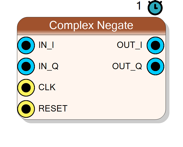
Introduction
The Complex Negate block outputs the arithmetic negation of the complex input sample:
OUT_I[n] = -IN_I[n]
OUT_Q[n] = -IN_Q[n]
Equivalently, with X = IN_I + j*IN_Q,
OUT = -X = X * exp(j*pi)
Negation rotates the phasor by 180 degrees (arg(OUT) = arg(X) + pi)
while leaving the magnitude unchanged. Data is signed two’s
complement.
Pin Description
Properties
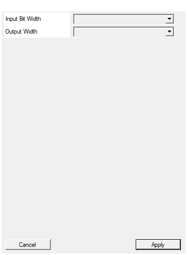
Bit width of each I/Q sample (signed).
Bit width of each signed I / Q input sample. Range 4 to 32, default 16. The output width isInputSize + 1.
Default: 16
Options: 4 5 6 7 8 9 10 11 12 13 14 15 16 17 18 19 20 21 22 23 24 25 26 27 28 29 30 31 32
Max = InputSize+1 (full precision, holds -(-2^(N-1))). Same as input = InputSize (no growth; SATURATED if the negated value exceeds the input range).
Default: Max (In+1)
Options: Max (In+1) Same as input
Usage
Bit widths
Data is signed two’s complement.
IN_I,IN_Q: signedInputSizebits.OUT_I,OUT_Q: signedInputSize + 1bits.
The output carries one extra bit because negating the most-negative value
(-2^(InputSize-1)) does not fit in InputSize bits; the guard bit keeps
the result exact for every input. Truncate downstream if you need to
return to InputSize bits.
Latency and throughput
#pragma HLS PIPELINE II=1: one sample pair per clock.- 1-clock latency.
- All data ports use the
ap_noneinterface (no ready/valid handshake); the core is free-running (ap_ctrl_none).
Reset
RESET is the HLS synchronous reset (ap_rst).
Typical applications
- Sign inversion of one branch of a differential / balanced datapath.
- 180-degree phase shift of a baseband phasor.
- Building block :
A - Bcan be formed asA + negate(B).
Resources & Timing
-
Latency: 1 clock cycle
-
Throughput: 1 sample per clock (II=1)
No multipliers or DSPs: two negations only. Implemented with Vitis HLS. Free-running core (ap_ctrl_none), no handshake logic.