Sync In
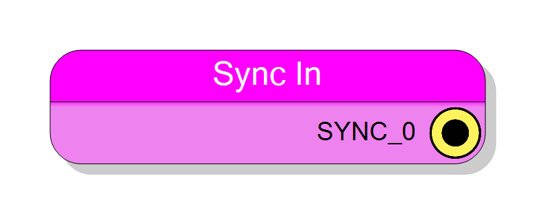
Board pin block that brings one of the three DT5560 front-panel SYNC input connectors into the diagram as a 1-bit signal. One concurrent assignment, no register, no synchroniser - the level arrives raw from the pin. DT5560 only.
Introduction
Principle of Operation
The DT5560 has three SYNC input connectors on the front panel. Sync In makes one of them visible in the diagram as an ordinary 1-bit source you can wire anywhere.
One block owns one connector, chosen with the Sync Pin property; place three blocks to read all three.
Its mirror image is Sync Out. Inputs and outputs are separate physical pins on the DT5560 - this is not a bidirectional port, and a Sync In block cannot drive anything.
Pin Description
Level present on the selected SYNC input connector, seen by the diagram as a source.
The pin is named after the selected connector: with SyncPin = SYNC_2
the pin is called SYNC_2. RedesignIfChanged is set on the property,
so changing the connector renames the pin and rebuilds the symbol -
wires to the old pin name are not preserved.
Asynchronous and unregistered. Synchronise it into your clock domain before use.
The assignment is emitted unconditionally (no unconnected-pad guard), so wire it.
Properties
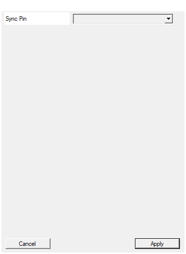
Set sync pin to use for this block
Which of the three DT5560 SYNC input connectors this block reads. The choice determines the pin name, the pad name and the board signal.
| Value | Board signal | Package pin |
|---|---|---|
SYNC_0 |
SYNC_0_IN |
B1 |
SYNC_1 |
SYNC_1_IN |
A2 |
SYNC_2 |
SYNC_2_IN |
A3 |
RedesignIfChanged is set - changing it rebuilds the symbol with a
differently named pin. It can be changed after the block is created.
Default: SYNC_0
Default: SYNC_0
Options: SYNC_0 SYNC_1 SYNC_2
⚙️ Detailed Operation
What the block compiles to
The pin name, the pad name and the source signal all follow the Sync Pin
property. For the default SYNC_0 the plug-in emits:
<your signal> <= SYNC_0_IN;
plus one informational line in the compiler output:
Generating HDL code for <designator>
No process, no generic, no register map entry, no SciSDK endpoint.
The board side
On the DT5560 the three sources are 1-bit vectors declared in the board’s top-level template, each fed straight from a top-level input port with no buffer primitive and no flip-flop:
vhdl
signal SYNC_0_IN : std_logic_vector(0 downto 0) := "0";
...
SYNC_0_IN(0) <= SYNC_0_INb;
SYNC_1_IN(0) <= SYNC_1_INb;
SYNC_2_IN(0) <= SYNC_2_INb;
constrained as single-ended 1.8 V CMOS inputs:
| Sync Pin | Board signal | Top-level port | Package pin | I/O standard |
|---|---|---|---|---|
SYNC_0 |
SYNC_0_IN |
SYNC_0_INb |
B1 | LVCMOS18 |
SYNC_1 |
SYNC_1_IN |
SYNC_1_INb |
A2 | LVCMOS18 |
SYNC_2 |
SYNC_2_IN |
SYNC_2_INb |
A3 | LVCMOS18 |
The same connectors under another name
The DT5560 board also publishes these three connectors to the generic
board-pin blocks as LEMO_IN_0..2: the board plug-in’s CompileIO handler
for a Digital Input named LEMO_IN_n emits the same
<signal> <= SYNC_n_IN; line. Reading one connector through both routes is
harmless - they are two readers of one signal, not two drivers - but it is a
good way to confuse yourself. Pick one route and stay with it.
Timing
Pure wiring: zero latency through the block, no clock, no reset, no debouncing and no minimum pulse width enforced by the firmware. A pulse narrower than one period of your clock may be missed entirely by the synchroniser you add downstream.
Typical use
- External trigger, gate or veto from another module.
- Run/stop or arm signal daisy-chained from a master board.
- Common start distributed to several DT5560s.
Board availability
DT5560 only. SupportedBoard is GUID_BASED with a single entry,
C7F960A5-8051-45F0-B793-8899650BAB9D, the board GUID declared by the DT5560
board plug-in (boards/ni/board_DT5560/bDT5560.vb). The block does not appear
in the toolbox on any other board, and no other board plug-in provides a
SYNC_n_IN signal for it to read.
The R5560 and R5560SE boards also have three SYNC lines, but they are LVDS and carry a different signal name - use System Sync there.