
Deserializer (Serial to Parallel)
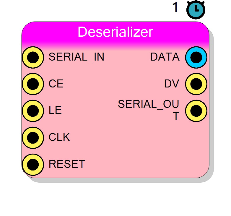
Converts serial bit stream to parallel data. Shifts in bits from SERIAL_IN one per clock cycle while CE=1, then outputs complete parallel word on DATA. Supports MSB-first or LSB-first bit order. Latency: N clock cycles where N is Parallel Width.
Introduction
This block converts serial data to parallel by shifting in bits one per clock cycle and assembling them into a parallel word. Useful for receiving serial communications.
Pin Description
Properties
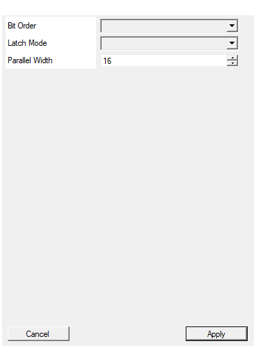
Set the order of the serialized bit
Bit reception order: MSB FIRST or LSB FIRST.Default: MSB FIRST
Options: MSB FIRST LSB FIRST
Select if latch output on latch or after the Parallel Width bits count from STREAM_START signal
Default: LATCH OUTPUT
Options: LATCH OUTPUT COUNT BITS
Set the size in bits of the output deserialized parallel word width
Parallel word width. Range: 2-65535 bits.Default: 16
Range: 2 – 65535
Functional description
Operation sequence:
- Assert CE=1 to enable shifting
- Input bits arrive on SERIAL_IN, one per clock cycle
- After N clock cycles, parallel word appears on DATA
Bit order
- MSB FIRST: First bit received becomes MSB of output word
- LSB FIRST: First bit received becomes LSB of output word
Timing
Latency: N clock cycles (where N = Parallel Width). Shift rate: 1 bit per clock cycle.
Typical use cases
- Serial communication receivers (SPI, UART)
- Bit-serial data recovery
- Data width conversion