
FFT TM Realtime
TRUE gapless realtime FFT for Time-Multiplexed signals. Polyphase architecture: R parallel Xilinx xfft cores (N/R points each, pipelined streaming) plus a multiplier-free R-point DIT recombination stage. Sustains R samples per clock continuously: DV stays high without gaps in steady state. TM factors 2 and 4.
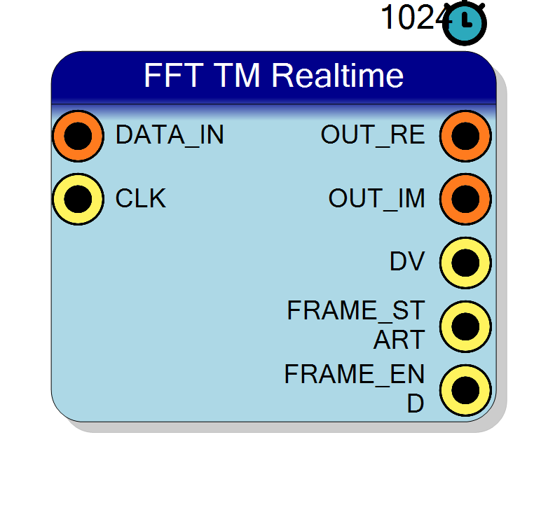
Introduction
The block computes a continuous stream of $N$-point FFTs on a TM input
($R$ samples per clock), producing $R$ frequency bins per clock with
no dead cycles: frames are processed back to back and DV stays
high continuously in steady state.
Internally the TM lanes are used directly as the polyphase components of a decimation-in-time split:
$$ X[k + q\tfrac{N}{R}] = \sum_{r=0}^{R-1} W_R^{rq}, W_N^{rk}, X_r[k] $$
where $X_r$ is the $N/R$-point FFT of lane $r$ (one Xilinx xfft core per lane, pipelined streaming = inherently gapless), $W_N^{rk}$ are ROM twiddles (16 bit) applied with one complex multiplier per lane $r \ge 1$, and the outer sum for $R = 2, 4$ uses only $\pm 1 / \pm j$: no multipliers in the recombination.
This custom architecture replaces the Vitis SSR FFT library, which was measured at only 11-24% sustained throughput (frame-serialized by design) on every tool version 2020.2..2025.1.
Pin Description
Properties
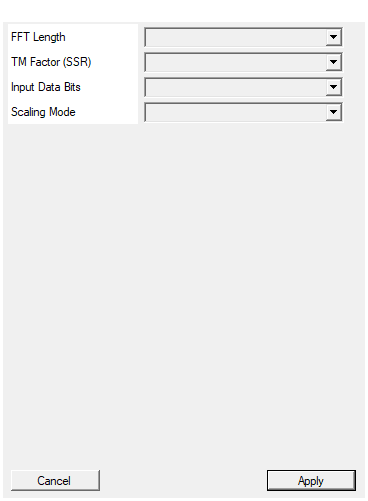
Number of points in the FFT transform (must be power of 2)
Transform length N (64..16384, power of 2).Default: 1024
Options: 64 128 256 512 1024 2048 4096 8192 16384
Time Multiplexing factor (samples per clock). 2 or 4 (multiplier-free recombination).
TM factor R: 2 or 4 only. These factors keep the recombination stage multiplier-free ($W_R^{rq} \in {\pm 1, \pm j}$).Default: 4
Options: 2 4
Bit width of each input sample (8-24 bits)
Input sample width (8..24, signed).Default: 16
Options: 8 9 10 11 12 13 14 15 16 17 18 19 20 21 22 23 24
No Scaling: full bit growth (InputBits + log2(N) + 1). Grow to Max: saturated to 27 bits. Scale: output divided by N, InputBits wide (saturated).
- No Scaling: full bit growth, output = InputBits + log2(N) + 1 bits per component (saturating, capped at 32).
- Grow to Max: same arithmetic, saturated to 27 bits.
- Scale: output divided by N (right shift), InputBits wide, saturating.
Default: No Scaling
Options: No Scaling Grow to Max Scale
How to read the output
Every $N$ input samples the block emits one complete $N$-point
spectrum, spread over $N/R$ consecutive clock cycles and $R$ TM lanes.
Counting DV cycles from FRAME_START (call the count $k$,
$k = 0 \ldots N/R-1$), output lane $q$ carries frequency bin
$k + q \cdot N/R$. Each lane is therefore one contiguous $1/R$
slice of the spectrum, in natural bin order:
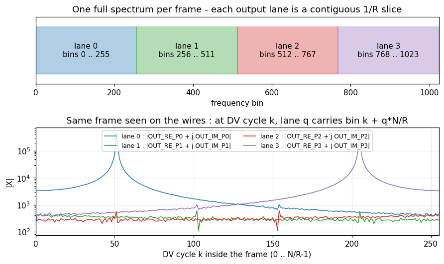
The lower plot above is real simulation data ($N=1024$, $R=4$, sine input at $f = 0.05,f_s$): all four lanes sweep their slice simultaneously, so at DV cycle 51 lane 0 shows the tone (bin 51) while lane 3, at cycle 205, shows its conjugate image (bin $973 = 205 + 768$).
Frame markers
FRAME_START is a one-cycle pulse aligned with the first DV cycle of
each frame (the cycle carrying bin 0); FRAME_END pulses on the last
cycle (the one carrying bins $qN/R - 1$). One frame = $N/R$ clock
cycles = $N$ input samples. Since frames are back to back,
FRAME_END of frame $j$ is immediately followed by FRAME_START of
frame $j+1$ on the next cycle. Use FRAME_START to reset your bin
counter $k$ - no free-running counter alignment is needed.
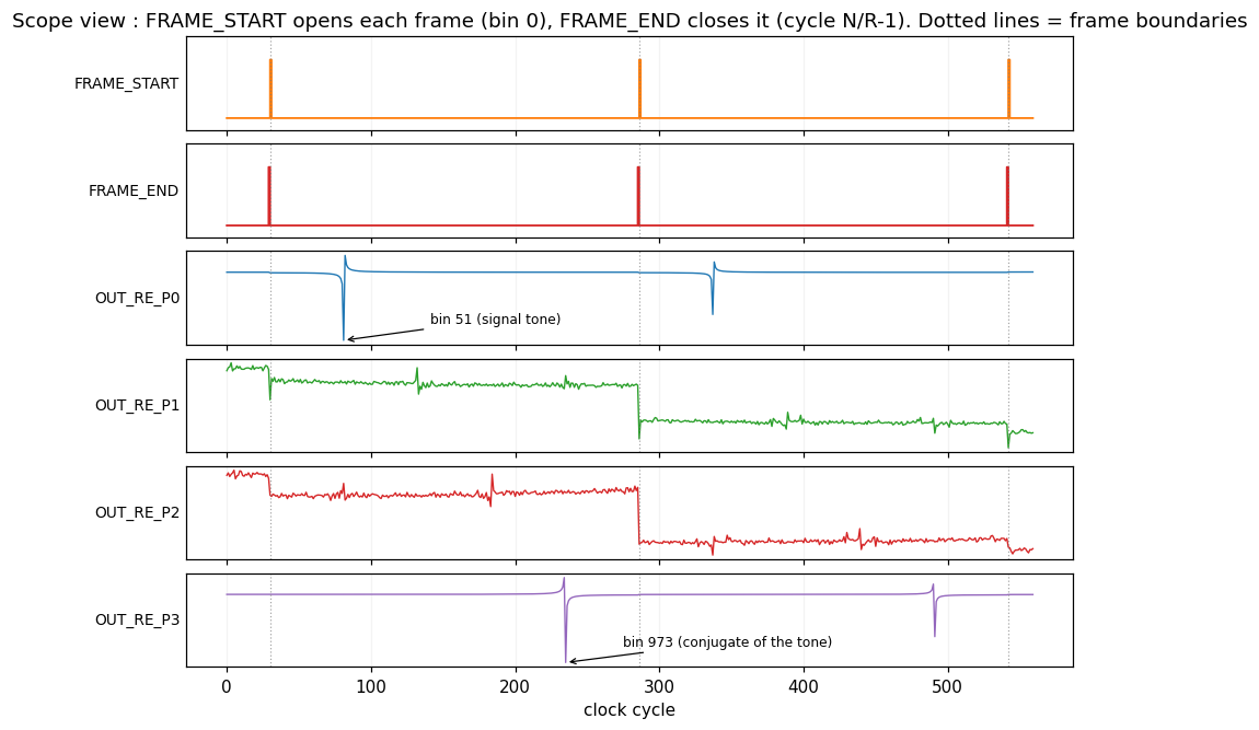
OUT_RE/OUT_IM of a single lane taken alone look odd on a scope:
the phase of each bin rotates rapidly from bin to bin and from
frame to frame (it depends on the block alignment of the input), so
the real and imaginary parts oscillate in sign. This is normal: the
spectrum information is in the complex pair. Compute per bin:
- magnitude: $|X| = \sqrt{\text{OUT_RE}^2 + \text{OUT_IM}^2}$ (shift-invariant, what you normally want)
- phase: $\angle X = \operatorname{atan2}(\text{OUT_IM}, \text{OUT_RE})$
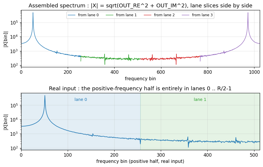
For a real input signal the spectrum is conjugate-symmetric ($|X[N-b]| = |X[b]|$), so lanes $0 \ldots R/2-1$ already contain the whole positive-frequency half: with $R = 4$ you can ignore lanes 2-3 (or use them as a consistency check), with $R = 2$ ignore lane 1. The frequency of bin $b$ is $f_b = b \cdot f_s / N$ where $f_s$ is the full (pre-TM) sample rate.
Latency and throughput
- Throughput: R samples in / R bins out every clock, sustained.
- Latency: dominated by the xfft cores (roughly $2 \cdot N/R$ clocks plus pipeline overhead); DV goes high once the first frame emerges and never drops afterwards.
Resources
- $R$ xfft cores of $N/R$ points (unscaled, pipelined streaming, natural order).
- $R-1$ complex multipliers (4 DSP each with 16-bit twiddles).
- $R-1$ twiddle ROMs of $N/R$ x 32 bit (BRAM).
- Recombination: adders only.