
Petiroc Analog
Analogue readout engine for one PETIROC-2A on the DT5550W. On a trigger it clocks the ASIC’s analogue multiplexer through its 32 channels, digitises each held charge with the board ADC through a 32-tap moving-average filter, and publishes the result twice - as a serial channel-by-channel stream and as 32 parallel energy/hit pairs latched at the end of the scan.

Introduction
Principle of Operation
In analogue mode the PETIROC-2A holds the peak charge of all 32 channels in
its internal analogue memories and presents them, one at a time, on a single
analogue output. A shift register inside the chip selects which channel is
presented: a token is injected on SRIN and walked along by SCLK. On the
DT5550W that analogue output is digitised by an external ADC whose 16-bit
result arrives at the FPGA as PETIROC_<ASIC>_ADC_ENERGY.
This block owns the whole sequence:
TRIG ─► inject token on SRIN
├─ for 36 shift steps:
│ SCLK low (CLKDIV+1 clocks) ← sample the filtered ADC here
│ SCLK high (CLKDIV+1 clocks)
│ advance (1 clock)
└─ latch 32 energies + 32 hits, pulse P_DV, replay the RAZ/VAL reset
The ADC conditioning chain
The raw ADC word is never published. Every clock the block computes
$$ f[n] = \mathrm{0x3FFF} - \mathrm{ADC_IN}[n] $$
(an inversion against a 14-bit full scale, because the ASIC’s analogue output swings downwards), pushes it into a shift register and maintains a running sum
$$ \mathrm{acc}[n] = \mathrm{acc}[n-1] + f[n-1] - f[n-32] \quad\Rightarrow\quad \mathrm{acc}[n] = \sum_{k=1}^{32} f[n-k] $$
The published value is acc(20 downto 5), i.e. the sum divided by 32 - a
plain 32-tap boxcar average of the inverted ADC stream. This is what both
S_ENERGY / P_E_<i> and the free-running monitor M_ENERGY carry. The
filter runs continuously, it is not reset between events, so the value latched
for a channel is the average of the last 32 ADC samples taken while that
channel was selected - which is why the readout must be slow enough for the
multiplexer to settle.
Pin Description
TS_OUT at the
trigger and held for the event. Purely a pipeline stage, the block does
not interpret the value.
TS0_OUT at the trigger.
OR_CHARGE of the Petiroc Trigger block.
RAZ_CHN / VAL_EVT reset sequence. Evaluated every
clock, outside the state machine, so it wins over any state. No output is
published for the aborted event.
TS_IN frozen at the trigger, stable for the
whole readout and until the next trigger. Pair it with P_DV.
TS0_IN frozen at the trigger.
S_DV. Counts the ASIC shift
steps after the discarded first one.
0x3FFF - ADC for the
channel named by S_CHID, valid with S_DV. Larger value = larger
charge (the inversion is already applied).
S_ENERGY, valid with S_DV. Tells you whether that channel
was over the charge threshold, independently of the digitised amplitude.
2·CLKDIV+3 clocks. Emitted at the sampling instant, one clock
before SCLK rises.
P_DV,
held until the next event. Same value that channel 0 carried on
S_ENERGY.
P_E_0, valid with P_DV.
P_E_0.
P_H_0.
P_E_0.
P_H_0.
P_E_0.
P_H_0.
P_E_0.
P_H_0.
P_E_0.
P_H_0.
P_E_0.
P_H_0.
P_E_0.
P_H_0.
P_E_0.
P_H_0.
P_E_0.
P_H_0.
P_E_0.
P_H_0.
P_E_0.
P_H_0.
P_E_0.
P_H_0.
P_E_0.
P_H_0.
P_E_0.
P_H_0.
P_E_0.
P_H_0.
P_E_0.
P_H_0.
P_E_0.
P_H_0.
P_E_0.
P_H_0.
P_E_0.
P_H_0.
P_E_0.
P_H_0.
P_E_0.
P_H_0.
P_E_0.
P_H_0.
P_E_0.
P_H_0.
P_E_0.
P_H_0.
P_E_0.
P_H_0.
P_E_0.
P_H_0.
P_E_0.
P_H_0.
P_E_0.
P_H_0.
P_E_0.
P_H_0.
P_E_0.
P_H_0.
P_E_0.
P_H_0.
P_E_* / P_H_* pairs and the frozen timestamps are simultaneously
valid. One pulse per accepted trigger.
0x3FFF - ADC_IN, free-running, independent of the state machine. Wire it
to an oscilloscope block to watch the multiplexed analogue signal and to
check that the readout is slow enough for each channel to settle.
SCLK line driven to the ASIC.
Useful as a trigger/qualifier when looking at M_ENERGY on a scope block.
SRIN line driven to the ASIC.
High from the trigger until the last shift step.
Properties
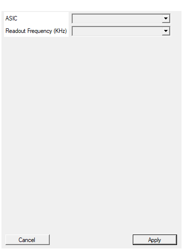
Select the ASIC to be connected to the Endpoint
Selects the PETIROC-2A this readout engine is bound to. The letter is
pasted into the board-support signal names emitted by CompileHDL:
PETIROC_<ASIC>_ADC_ENERGY (16-bit ADC word),
PETIROC_<ASIC>_CHARGE_HIT_s, PETIROC_<ASIC>_SRIN_s,
PETIROC_<ASIC>_SCLK_s, <ASIC>_VAL_EVT_s, <ASIC>_RAZ_CHN_s.
| Value | Board ADC channel wired to ADC_IN |
|---|---|
A |
ADC_A1 |
B |
ADC_A3 |
C |
ADC_A5 |
D |
ADC_A7 |
Hidden (isVisible = False): the board plug-in sets it when the block is
placed.
Default: A
Default: A
Options: A B C D
Set the readout frequency for the chip. Value higher than 500KHz reduce the quality of the measure
Nominal rate of the analogue multiplexer shift clock, in kHz. It is turned
into the CLKDIV generic as CLKDIV = 160000 / ReadoutFrequency, and the
state machine then spends CLKDIV+1 clocks per half bit, so the true
shift rate is f_clk / (2·CLKDIV + 3) - see the alert in the description
about the factor-two difference and the hard-coded 160 MHz assumption.
| Setting (kHz) | CLKDIV |
Real shift rate at 160 MHz | Scan duration |
|---|---|---|---|
| 1 | 160000 | ≈ 0.5 kHz | ≈ 72 ms |
| 10 | 16000 | ≈ 5 kHz | ≈ 7.2 ms |
| 50 | 3200 | ≈ 25 kHz | ≈ 1.4 ms |
| 100 | 1600 | ≈ 50 kHz | ≈ 720 µs |
| 200 | 800 | ≈ 100 kHz | ≈ 360 µs |
| 400 | 400 | ≈ 199 kHz | ≈ 181 µs |
| 500 | 320 | ≈ 249 kHz | ≈ 145 µs |
| 1000 | 160 | ≈ 496 kHz | ≈ 73 µs |
| 2500 | 64 | ≈ 1.22 MHz | ≈ 29 µs |
| 4000 | 40 | ≈ 1.93 MHz | ≈ 19 µs |
| 5000 | 32 | ≈ 2.39 MHz | ≈ 15 µs |
The block’s own description warns that “value higher than 500 KHz reduce
the quality of the measure”: above that the 32-tap moving average has not
yet flushed the previous channel when the sample is taken, so adjacent
channels bleed into each other. Scan duration above is
36 × (2·CLKDIV+3) clocks and sets the dead time per event.
Hidden (isVisible = False) in the current version.
Default: 500
Default: 500
Options: 1 10 50 100 200 400 500 1000 2500 4000 5000
⚙️ Detailed Operation
Readout clock rate
CompileHDL passes one generic:
Component.AddGenericInteger("CLKDIV", 160000 / ReadoutFrequency)
with ReadoutFrequency in kHz, so CLKDIV = 160000 / f_readout[kHz]
(500 kHz → 320). The state machine spends CLKDIV+1 clocks with SCLK low,
CLKDIV+1 clocks with SCLK high and one more clock to advance, so the real
shift-register period is
$$ T_{bit} = (2,\mathrm{CLKDIV} + 3)\ \text{clock cycles},\qquad f_{bit} = \frac{f_{clk}}{2,\mathrm{CLKDIV}+3} $$
A full event therefore takes about
36 × (2·CLKDIV+3) clocks (≈ 23 150 clocks ≈ 145 µs at the default settings),
plus 31 clocks for the channel-reset sequence.
The 36-step scan
| Step | What happens |
|---|---|
| trigger | SRIN raised (token injected), BUSY high, TS_IN/TS0_IN latched, bit counter = 35, skip flag set |
| steps 1…36 | one SCLK cycle each; the filtered ADC value and CHARGE_HIT are sampled one clock before SCLK rises |
| step 1 | discarded (the skip flag): the multiplexer output is not valid yet |
| steps 2…33 | channels 0…31 → serial stream and internal buffer |
| steps 34…36 | sampled into the buffer but never published |
| end | 32 energy/hit pairs driven onto P_E_*/P_H_*, P_DV pulsed one clock, SRIN lowered, reset sequence restarted |
SRIN is held high from the trigger until the last shift step, so the token
is present on the ASIC shift register for the whole scan.
Two output styles, same data
- Serial (
S_CHID,S_ENERGY,S_HIT,S_DV): oneS_DVpulse per channel, 32 pulses per event, spaced byT_bit.S_CHIDcarries the channel index 0…31. Cheap in logic - feed it straight into a histogrammer, a spectrum block or a list-mode packet builder. - Parallel (
P_E_0…31,P_H_0…31,P_DV): all 32 energies and hit flags presented simultaneously, oneP_DVpulse per event, at the end of the scan. Costs 544 wires but lets you do per-event logic (sum, maximum, centroid, multiplicity) in one clock.
Both are produced from the same buffer, so they always agree; use whichever fits the downstream block, or both.
The RAZ_CHN / VAL_EVT reset sequence
Identical to the one in Petiroc Digital. After reset, after every scan and
on every REJECT, an 8-bit counter is loaded with 0x1F and counts down:
| Counter value | RAZ_CHN |
VAL_EVT |
|---|---|---|
0x1F |
1 |
0 |
0x15 |
0 |
0 |
0x07 |
1 |
0 |
0x00 (stops) |
1 |
1 |
a 14-clock low pulse on RAZ_CHN that clears the analogue memories, then
VAL_EVT high (the chip is armed) until the next event.
Timestamp pass-through
TS_IN/TS0_IN are copied to TS_OUT/TS0_OUT at the trigger and held
for the whole readout. The block does not generate time codes of its own - it
just freezes whatever counters you feed it so the energies and the time of the
event stay together through the rest of the pipeline. Leave them open if you
do not need them.
Monitor outputs
M_ENERGY, M_CLK and M_DIN are unconditional copies of the internal
filtered ADC value, the shift clock and the token line. They are free-running
(not gated by the state machine), which makes them useful for an oscilloscope
block: put M_ENERGY on a scope to see the multiplexed analogue baseline in
real time and to set the ReadoutFrequency slow enough that each channel’s
plateau is flat before it is sampled.
Failure modes
There is no ValidateSettings and no compile-time check on this block; the
only message it prints is the informational Generating HDL code For <designator>. Symptoms to recognise in hardware:
- All channels identical / smeared – readout too fast: the 32-tap average
still contains samples from the previous channel. Lower
ReadoutFrequency. - Energies offset by one channel – the discarded first step is what aligns the token with channel 0; if the ASIC shift register is configured differently the whole map shifts.
BUSYstuck high – the state machine never left the scan; assertREJECT(or the global reset) to force it back to idle.
Resources & Timing
-
Latency: One scan = 36 × (2·CLKDIV + 3) clock cycles from the trigger to P_DV, plus 31 clocks of channel-reset sequence before the block is armed again.
-
Throughput: One event per scan; at the default 500 kHz setting on a 160 MHz clock that is ≈ 145 µs of dead time per event (≈ 6.9 kevents/s maximum).
S_DVpulses arrive one per2·CLKDIV+3clocks during the scan;P_DVpulses once at the end.- The ADC moving-average filter is 32 taps deep and never reset, so it also imposes a 32-clock settling time on
M_ENERGYafter any step on the analogue input.