
List DMA
High-throughput list block for the Ultraspectra board. It behaves like the standard List — write a word, read a stream — but its read port is 64 bits wide and is drained by a dedicated AXI DMA engine straight into DDR instead of through the register bridge. One DMA engine is generated per block, and the DMA channel is assigned automatically by the board at compile time.
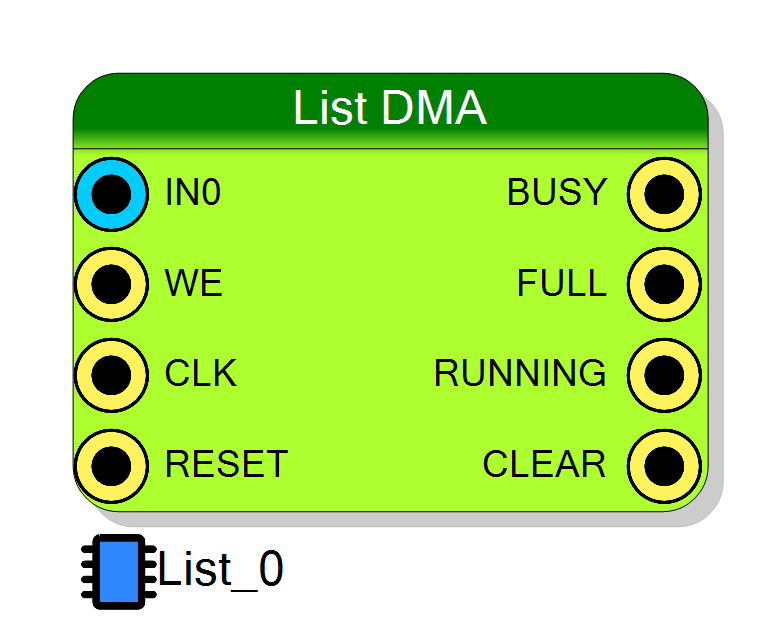
Introduction
Principle of Operation
The List DMA block is a FIFO you write words into and software reads a byte
stream out of. Functionally it is the standard List: the same WE / FULL /
BUSY / RUNNING / CLEAR contract, the same CONFIG / STATUS registers, the
same “you decide what the bits mean” raw payload.
What is different is the road the data takes out of the FPGA.
standard List : FIFO ──32 bit──► register bridge ──► PS ──► PC
List DMA : FIFO ──64 bit──► AXIS reader ──► AXI DMA (S2MM, SG) ──► DDR
A standard list is emptied one 32-bit word at a time by the processor reading a register window. A List DMA is emptied by an AXI DMA engine in scatter-gather mode, 64 bits per beat, writing directly into a ring of buffers in DDR through the high-performance port. The processor only has to hand out descriptors.
What the compiler builds around this block
Dropping this block into a design makes the board plugin generate, at compile time:
- a
list_fifo_to_axisreader that pulls the 64-bit FIFO port and turns it into an AXI-Stream, enabled by the list’s own run bit; - a dedicated AXI DMA (S2MM only, scatter-gather, 64-bit stream) instantiated in the block design;
- the interconnect, address map and clock/reset wiring to the PS high-performance port.
There is no stream arbiter: N DMA lists produce N DMA engines.
The DMA channel is not yours to choose
The channel number ends up in RegisterFile.json as the DMAChannel field next
to UseDMA: true, and SciSDK uses it to find the DMA registers. In the design
itself, CompileSDK emits JSON only — no C or Python helper library is
generated for this block.
Where it can be used
- Ultraspectra only. The block declares the Ultraspectra board GUID and is hidden everywhere else.
- Top page only. The DMA reader is wired into the top-level architecture, so the block cannot be placed on a subpage. (This is also what keeps the endpoint address used for channel ranking equal to the address published in the JSON.)
Pin Description
Data input – the word written into the FIFO, Wordsize bits wide.
Sampled on the rising edge of CLK whenever the write is accepted
(CONFIG[0] AND WE AND NOT FULL).
The payload is opaque to the block: it is delivered to DDR byte for byte, least significant 64-bit slice first.
Write enable – while high, one word is taken from IN_0 per clock.
The write is dropped, without notice, if the list is stopped
(CONFIG[0] = 0) or if FULL is high.
Write clock – the acquisition-side clock of the FIFO. Defaults to the project acquisition clock when left unconnected.
The read side runs on the board bus clock (100 MHz on this board); the FIFO is the crossing between the two.
CONFIG[1]) and shows up
on the CLEAR output.
Defaults to the project global reset when left unconnected.
Not accepting data – BUSY = NOT CONFIG[0] OR FULL.
High while the list is stopped or the FIFO is full. This is the signal to use for back-pressuring your data source: it covers both “software has not started me” and “I have no room”.
Run indicator – RUNNING = CONFIG[0], i.e. it mirrors the software
enable bit. The same bit enables the generated DMA reader.
Undriven in simulation — see the simulation note.
Clear pulse – CLEAR = CONFIG[1] OR RESET. Use it to reset the upstream
logic in step with the list FIFO being cleared.
Undriven in simulation — see the simulation note.
Properties
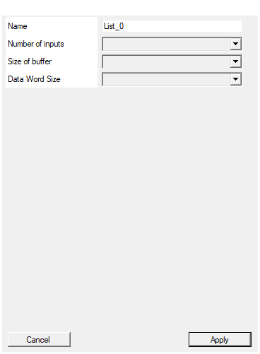
Set the name of the endpoint
Name of the memory-mapped endpoint. It names the registers
(REG_<EndpointName>_STATUS_RD, REG_<EndpointName>_CONFIG_WR), the
board-generated read-out signals (BUS_<EndpointName>_…) and the entry in
RegisterFile.json.
It must be unique in the design. Note that the endpoint’s address — which follows from where it lands in the memory map — is what decides this block’s DMA channel number relative to the other DMA lists.
Default: List_0
Default: List_0
Set the number of input to the virtual block
Number of input pins fed into the FIFO in parallel. It is exposed as a hidden
property and is effectively fixed at 1 — the symbol is built with a single
IN_0 pin and the value is published as Channels in RegisterFile.json.
Default: 1
Default: 1
Options: 1 2 4 8 16 32 64 128
Size of the readout buffer. Buffer must be large enought to compensate readout bus stalls.
FIFO depth in written words (the fifolength generic).
Available values: 128, 256, 512, 1024, 2048, 4096, 8192, 16384, 32768, 65536.
This is the burst tolerance between your acquisition clock and the DMA: it is
how much data can arrive faster than the DMA drains it before FULL asserts
and words start being lost. Note that the storage cost scales with
BufferSize × Wordsize, so a deep buffer at 256-bit words is expensive.
Default: 1024
Default: 1024
Options: 128 256 512 1024 2048 4096 8192 16384 32768 65536
Set the data word size in bits. Must be a multiple of 64 (the DMA stream is 64 bit wide)
Width of IN_0 in bits, i.e. the size of one written word (the bitsize
generic).
| Value | DMA beats per word |
|---|---|
| 64 | 1 |
| 128 | 2 |
| 256 | 4 |
Only multiples of 64 are offered: the FIFO read port is fixed at 64 bits and
the asymmetric XPM FIFO needs a power-of-two width ratio. The value is
published in RegisterFile.json as WordSize = Wordsize / 32 (in 32-bit
units).
Changing it rebuilds the symbol.
Default: 64
Default: 64
Options: 64 128 256
⚙️ Detailed Operation
Datapath
┌──────────────────────── component (LISTMODULEDMA64) ────────────────────────┐
│ │
│ IN_0 ─────────►┌──────────────────────┐ │
│ (Wordsize) │ xpm_fifo_async │──64──► READ_DATA │
│ WE ───────────►│ write: Wordsize bit │──────► READ_DATAVALID │
│ CLK ──────────►│ read : 64 bit │◄───── READ_NEXT │
│ RESET ────────►│ depth: BufferSize │ │
│ └──────────────────────┘ │
│ BUSY FULL RUNNING CLEAR STATUS ◄─┘ ▲ CONFIG │
└──────────────────────────────────────────┼──────────┼──────────────────────-─┘
│ │
┌──── board plugin (generated) ────────────▼──────────┴──────────────────────┐
│ list_fifo_to_axis ──► AXI DMA (S2MM, scatter-gather, 64 bit) ──► HP0 ──► DDR
└────────────────────────────────────────────────────────────────────────────┘
The FIFO is a single xpm_fifo_async with asymmetric widths: the write side is
Wordsize × InputCount bits wide, the read side is fixed at 64. It runs in
standard (non-FWFT) mode with a read latency of one clock.
Write side
iWRITE = CONFIG[0] AND WE AND (NOT FULL)
A word is accepted only when the list is running, WE is high and the FIFO has
room. Writes presented while FULL is high are silently lost — there is no
overflow counter.
The status outputs are pure combinational functions of that state:
| Signal | Logic |
|---|---|
RUNNING |
CONFIG[0] |
BUSY |
NOT CONFIG[0] OR FULL |
FULL |
FIFO full flag |
CLEAR |
CONFIG[1] OR RESET |
Read side and the 64-bit constraint
One written word therefore becomes Wordsize / 64 DMA beats, emitted least
significant 64-bit slice first.
CONFIG register (write)
| Bit | Function |
|---|---|
| 0 | Run. 1 enables writes and enables the DMA reader. 0 stops both. |
| 1 | Force reset. Resets the FIFO and pulses the CLEAR output. |
CONFIG[0] is doing double duty here: besides gating the writes it is the
ENABLE of the generated list_fifo_to_axis reader (resynchronised inside the
reader), so clearing it also stops the DMA stream.
STATUS register (read)
| Bits | Meaning |
|---|---|
| 0 | Nearly empty — see the note below |
| 1 | Full |
| 7:2 | reserved, read as 0 |
| 31:8 | number of 64-bit words currently available on the read side |
Bits 31:8 come from the read clock domain through a bit-wise synchroniser, so
treat the count as an estimate, not as an exact instantaneous value. Bit 1 (FULL)
is taken directly from the write domain.
The generated reader and the DMA
The list_fifo_to_axis core the board instantiates for each DMA list:
| Parameter | Value | Meaning |
|---|---|---|
DATA_WIDTH |
64 | matches the list read port and the DMA stream |
PACKET_WORDS |
512 | beats per TLAST, i.e. 512 × 8 B = 4 KB per descriptor buffer |
IDLE_TIMEOUT |
12500 | idle clocks before a short packet is flushed — ≈ 125 µs at 100 MHz |
So a steady stream is cut into 4 KB descriptors, and a stream that dries up is flushed after roughly 125 µs instead of sitting in the reader indefinitely.
On this board everything in the path runs on one clock: FCLK_CLK0 (100 MHz) is
the bus clock, the list’s read clock and the DMA clock. The only clock-domain
crossing is the list FIFO itself, between CLK (your acquisition clock) and that
bus clock.
The DMA writes through the PS HP0 port, which is not cache coherent —
software must map the destination buffer non-cached (the usual u-dma-buf /
O_SYNC arrangement) and use a cyclic scatter-gather ring.
Software view
CompileSDK emits a JSON descriptor only. The entry in RegisterFile.json is a
ListModule with:
| Field | Value |
|---|---|
Type |
ListModule |
UseDMA |
true |
DMAChannel |
filled in by the board (-1 as written by the component) |
WordSize |
Wordsize / 32 — the word length in 32-bit units |
Channels |
InputCount |
Registers |
STATUS, CONFIG |
Apart from UseDMA / DMAChannel this is the same descriptor a standard list
produces, so the payload is read back the same way: as a raw byte stream that your
code casts to whatever structure you packed into IN_0.
// Example: one 64-bit word per event
#pragma pack(push, 1)
typedef struct {
uint32_t timestamp;
uint16_t energy;
uint16_t channel;
} EVENT_DATA; // 64 bits, matches Wordsize = 64
#pragma pack(pop)
Simulation
Compiler messages
| Message | Meaning |
|---|---|
Generating memory mapped component (DMA list): <endpoint> |
informational |
SDK starting code generation (JSON only) |
informational — confirms no C/Python library is produced |
SDK address undefined for <endpoint> |
error — the endpoint got no base address |
DMA List <endpoint> -> DMAChannel n (AXI DMA registers @ 0x…) |
the channel this block was assigned |
DMA list: cores\list_fifo_to_axis.vhd missing in … - the board support files are out of date (re-run copy_to_bin) |
error, see below |
DMA list: marker ##DMA_BD_REGION## missing in ZynqDesign.tcl - the board support files are out of date (re-run copy_to_bin) |
error, see below |
DMA list: markers ##DMA_*## missing in cores\Mars_ZX2_wrapper.vhd - the board support files are out of date (re-run copy_to_bin) |
error, see below |
DMA list: markers ##DMA_WRAPPER_*## missing in top_project_name.vhd - the board support files are out of date (re-run copy_to_bin) |
error, see below |
Quick reference
| Item | Value |
|---|---|
| Word size | 64, 128 or 256 bits |
| Buffer | BufferSize words |
| Read port | 64 bits, one AXI DMA per block |
| Max DMA lists per design | 4 |
| DMA channel | assigned automatically by endpoint address order |
| Registers | STATUS (read), CONFIG (write) |
| Destination | DDR, through PS HP0 (not cache coherent) |
| Board | Ultraspectra only, top page only |
Resources & Timing
- Throughput: One word per acquisition clock on the write side; the read side moves 64 bits per bus clock beat into DDR
- One
xpm_fifo_async(block RAM) ofBufferSize×Wordsizebits, plus two 32-bitxpm_cdc_array_singlesynchronisers forCONFIGandSTATUS. - Per block, the board additionally generates one
list_fifo_to_axisreader and one AXI DMA (S2MM, scatter-gather, 64-bit) in the block design, plus its share of the interconnect to the PS HP0 port. - Maximum 4 DMA lists per design; their AXI DMA register windows are at
0x43CA0000 + n × 0x10000, 64 KB each. - Ultraspectra board only; top page only (not available in subpages).