
Logic AND
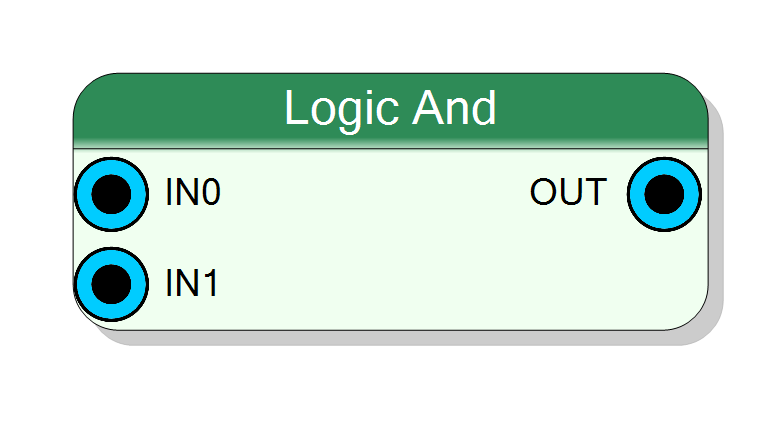
Bitwise AND operation. Performs logical AND between multiple inputs (2 to 1024). Output is 1 only when all corresponding input bits are 1. Effectively finds the minimum between input binary digits. Pure combinational logic (zero latency).
Introduction
This block performs a bitwise AND operation on multiple input signals (configurable from 2 to 1024 inputs). All inputs must have the same bit width.
The output is 1 (HIGH or True) if and only if all corresponding input bits are 1. If at least one input bit is 0 (LOW or False), the output will be 0.
The operation is purely combinational with zero clock latency:
$$ \mathrm{OUT} = \mathrm{IN}_0 \land \mathrm{IN}_1 \land \ldots \land \mathrm{IN}_N, $$
where $\land$ represents the logical AND operation and $N$ is the number of inputs.
Pin Description
Properties
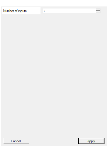
Set the number of input to the virtual block
Number of input signals to the AND gate. Range: 2 to 1024. This property is set during block creation and defines how many input pins the component will have.Default: 2
Functional description
The component implements a multi-input bitwise AND gate in VHDL. Each bit position of the output is the AND of all corresponding input bits:
$$ y[i] = x_0[i] \land x_1[i] \land \ldots \land x_N[i], $$
where:
- $x_k[i]$ → bit $i$ of input $k$
- $y[i]$ → bit $i$ of the output
- $\land$ → logical AND operation
The AND gate is one of the fundamental building blocks in digital logic. It implements logical conjunction:
| IN0 | IN1 | OUT |
|---|---|---|
| 0 | 0 | 0 |
| 0 | 1 | 0 |
| 1 | 0 | 0 |
| 1 | 1 | 1 |
For multi-bit inputs, the operation is applied independently to each bit position. In another sense, the logic AND gate effectively finds the minimum between the input binary digits.
Example
Given two 8-bit inputs:
- IN0:
10110011 - IN1:
11010101
Output: 10010001 (bitwise AND of all inputs)
Mathematical background
The AND operation is one of the three basic Boolean operations (AND, OR, NOT). It implements logical conjunction:
$$ 0 \land 0 = 0 $$ $$ 0 \land 1 = 0 $$ $$ 1 \land 0 = 0 $$ $$ 1 \land 1 = 1 $$
In Boolean algebra, the AND operation has the following properties:
- Commutativity: $x \land y = y \land x$
- Associativity: $(x \land y) \land z = x \land (y \land z)$
- Identity element: $x \land 1 = x$
- Annihilator: $x \land 0 = 0$
Timing
The component is purely combinational with zero latency:
| Property | Latency (clock cycles) |
|---|---|
| Logic AND | 0 |
The output changes immediately (after propagation delay) when any input changes.
Typical use cases
- Masking operations in data processing
- Implementing enable/disable logic
- Building blocks for more complex Boolean functions
- Bitwise operations in arithmetic circuits
- Control signal gating