
I2C Master
Implements an I2C (Inter-Integrated Circuit) master controller for communicating with I2C slave devices. Supports both memory-mapped (PC control) and FPGA-controlled operation modes.
Introduction
The I2C Master block implements an I2C (also called IIC or TWI - Two Wire Interface) master controller for communicating with I2C slave devices such as EEPROMs, temperature sensors, ADCs, DACs, and other peripherals.
I2C is a synchronous, multi-master, multi-slave serial communication protocol that uses only two wires:
- SDA (Serial Data Line): Bidirectional data line
- SCL (Serial Clock Line): Clock signal generated by the master
The block supports two operation modes:
- Memory Mapped: Transactions controlled entirely from PC software
- FPGA: Transactions controlled by FPGA logic with full pin access
Pin Description
Acknowledgment to send after reading a byte.
- HIGH: Send ACK (continue reading)
- LOW: Send NACK (end of read sequence) FPGA mode only.
Acknowledgment received from slave after writing.
- HIGH: Slave acknowledged (ACK)
- LOW: Slave did not acknowledge (NACK) FPGA mode only.
Ready signal indicating master is idle.
- HIGH: Ready for new operation
- LOW: Transaction in progress Wait for READY before starting new byte transfer. FPGA mode only.
Properties
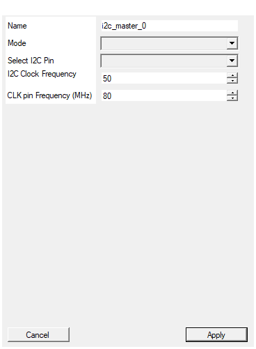
Set the name of the endpoint
Default: i2c_master_0
Select between memory mapped petipheral and FPGA control mode. In memory mapped mode the core can be controlled only via register from PC
Default: Memory Mapped
Options: FPGA Memory Mapped
Select the I2C pin to be used by the code.
Default: ANCON
Options: ANCON DIGCON_A DIGCON_B
Set SCL frequency for the I2C master
Default: 50
Range: 1 – 4000
Set the pin clock frequency in order to correcly calculate the scaler frequency
Default: 80
Range: 1 – 500
"IIC_SENSOR" generates SCI_REG_IIC_SENSOR_xxx.
Default: I2C_0.
Operation mode selection.
- Memory Mapped: PC software controls all I2C transactions
- FPGA: FPGA logic controls I2C with exposed pins Default: Memory Mapped.
Physical I2C bus connection on the board. Available options depend on hardware:
- ANCON: Analog connector I2C bus
- DIGCON_A: Digital connector A I2C bus
- DIGCON_B: Digital connector B I2C bus
- IIC: Internal I2C bus (DT5550W) Default: ANCON.
I2C clock frequency in KHz.
- Range: 1 to 4000 KHz
- Default: 50 KHz Common values: 100 (standard), 400 (fast mode). Note: Actual frequency depends on input clock and divider calculation.
Input clock frequency driving the I2C master. Used to calculate the clock divider for SCL generation.
- Range: 1 to 500 MHz
- Default: 80 MHz Must match the actual clock connected to the component.
Usage
I2C Protocol Overview
I2C communication follows a master-slave architecture where the master initiates all transactions:
Master Slave
│ │
│──── START condition ────────────────►│
│──── Slave Address (7/10 bit) + R/W ─►│
│◄─────────────── ACK ─────────────────│
│──── Data byte ──────────────────────►│ (Write)
│◄─────────────── ACK ─────────────────│
│◄──────────────── Data byte ──────────│ (Read)
│──── ACK/NACK ───────────────────────►│
│──── STOP condition ─────────────────►│
│ │
Key protocol elements:
| Element | Description |
|---|---|
| START | SDA goes LOW while SCL is HIGH - begins transaction |
| STOP | SDA goes HIGH while SCL is HIGH - ends transaction |
| ACK | Receiver pulls SDA LOW during 9th clock - acknowledgment |
| NACK | Receiver leaves SDA HIGH during 9th clock - no acknowledgment |
| Address | 7-bit (most common) or 10-bit slave address |
| R/W bit | 0 = Write to slave, 1 = Read from slave |
Operation Modes
Memory Mapped Mode
In Memory Mapped mode, the I2C master is controlled entirely through software register access. This is the simplest mode for PC-controlled communication.
Features:
- No FPGA pins exposed
- All control through SDK functions
- Ideal for configuration and calibration tasks
- Software handles the complete protocol
Typical use cases:
- Reading/writing EEPROM configuration
- Reading temperature sensors
- Configuring external ADCs/DACs
- Slow, non-time-critical communication
FPGA Mode
In FPGA mode, the I2C master exposes control and data pins for FPGA logic integration.
Features:
- Full control from FPGA fabric
- Byte-level transaction control
- Handshaking signals for synchronization
- Can be used for time-critical operations
I2C Transaction Examples
Writing a Byte to EEPROM
Transaction sequence:
1. START
2. Send device address + Write bit (0)
3. Wait for ACK
4. Send memory address high byte
5. Wait for ACK
6. Send memory address low byte
7. Wait for ACK
8. Send data byte
9. Wait for ACK
10. STOP
Timing diagram:
SCL: ─┐┌┐┌┐┌┐┌┐┌┐┌┐┌┐┌┐─┐┌┐┌┐┌┐┌┐┌┐┌┐┌┐┌┐─...
SDA: ─┘ ADDRESS + W └─┘ MEMORY ADDR └─...
START ACK ACK
Reading a Byte from EEPROM
Transaction sequence (Random Read):
1. START
2. Send device address + Write bit (0)
3. Wait for ACK
4. Send memory address high byte
5. Wait for ACK
6. Send memory address low byte
7. Wait for ACK
8. Re-START
9. Send device address + Read bit (1)
10. Wait for ACK
11. Read data byte
12. Send NACK (to end read)
13. STOP
Clock Configuration
The I2C clock frequency is derived from the input clock:
SCL_frequency = Input_Clock / (4 × Divider)
Where Divider = Input_Clock / (4 × SCL_frequency)
Common configurations:
| Input Clock | SCL Frequency | Divider |
|---|---|---|
| 80 MHz | 100 KHz | 200 |
| 80 MHz | 400 KHz | 50 |
| 100 MHz | 100 KHz | 250 |
| 100 MHz | 400 KHz | 62 |
I2C speed modes:
| Mode | Max Frequency | Typical Use |
|---|---|---|
| Standard | 100 KHz | Most devices |
| Fast | 400 KHz | Sensors, EEPROMs |
| Fast Plus | 1 MHz | High-speed devices |
FPGA Mode Pin Usage
When in FPGA mode, use the following sequence for a write operation:
1. Wait for READY = 1 (master idle)
2. Set DATA_OUT to the byte to send
3. Set START_BIT = 1 if this is first byte
4. Set STOP_BIT = 1 if this is last byte
5. Set WRITE_OP = 1
6. Wait for DV = 1 (operation complete)
7. Check STATUS for ACK/NACK
For a read operation:
1. Wait for READY = 1
2. Set READ_OP = 1
3. Set ACK_IN = 1 to acknowledge (more data coming)
4. Set ACK_IN = 0 for NACK (last byte)
5. Wait for DV = 1
6. Read DATA_IN for received byte
Available I2C Pins by Board
| Board | Available Pins |
|---|---|
| DT5550 | ANCON, DIGCON_A, DIGCON_B |
| DT5550W | IIC (HV Controller) |
Best Practices
- Pull-up resistors: I2C requires external pull-up resistors on SDA and SCL (typically 4.7kΩ)
- Bus capacitance: Keep total bus capacitance under 400pF for reliable operation
- Address conflicts: Ensure no two devices share the same I2C address
- Clock speed: Start with 100 KHz, increase only if needed and tested
- Error handling: Always check ACK/NACK responses in software
Resources & Timing
-
Latency: Variable (depends on transaction length and SCL frequency)
-
Throughput: 1 byte per ~90 SCL cycles (9 bits × 10 for protocol overhead)
I2C is a relatively slow interface; use for configuration and slow peripherals. For high-speed data transfer, consider SPI or parallel interfaces.