Understanding FPGA Devices
A comprehensive introduction to Field Programmable Gate Array (FPGA) technology. Covers the fundamental building blocks, internal architecture, programming concepts, and why FPGAs are ideal for real-time signal processing in scientific instrumentation.
What is an FPGA?
Field Programmable Gate Arrays (FPGAs) are integrated circuits that enable designers to program customized digital logic in the field. Unlike microprocessors that execute software instructions sequentially, FPGAs implement algorithms as physical circuits where all operations execute simultaneously.
FPGAs have been around since the 1980s and were originally conceived to give all design teams the ability to create custom logic. Compared to other ways of building hardware, FPGAs enable you to build exactly the hardware you need.
Key Characteristics
| Feature | Description |
|---|---|
| Reconfigurable | Can be reprogrammed to implement different circuits |
| Parallel | Thousands of operations execute simultaneously |
| Deterministic | Fixed, predictable timing (nanosecond precision) |
| Custom | Hardware tailored exactly to your algorithm |
| Field-upgradeable | Update functionality without changing hardware |
The Building Blocks of Digital Systems
You can build anything digital from three simple pieces:
Logic Gates
Logic gates perform the core functionality of digital circuits. They operate on electrical signals representing 0s and 1s. On their own, these simple operations do not do much, but when you put thousands or millions together, you can do something really powerful.
Basic Boolean Operations:
| Gate | Symbol | Function |
|---|---|---|
| AND | A · B | True only if both A and B are true |
| OR | A + B | True if either A or B is true |
| NOT | ¬A | Inverts the input (true becomes false) |
| XOR | A ⊕ B | True if A and B are different |
| NAND | ¬(A · B) | NOT AND - Universal gate |
| NOR | ¬(A + B) | NOT OR - Universal gate |
Truth Tables:
AND Gate OR Gate XOR Gate
A | B | Out A | B | Out A | B | Out
--|---|---- --|---|---- --|---|----
0 | 0 | 0 0 | 0 | 0 0 | 0 | 0
0 | 1 | 0 0 | 1 | 1 0 | 1 | 1
1 | 0 | 0 1 | 0 | 1 1 | 0 | 1
1 | 1 | 1 1 | 1 | 1 1 | 1 | 0
Registers (Flip-Flops)
Registers are simple devices that store pieces of data. Think of registers as short-term memory for placing data that you can access quickly. They keep whatever information is given to them until they are told to remember something new.
Key register concepts:
- D Flip-Flop: Stores one bit, updates on clock edge
- Clock: The heartbeat that synchronizes all operations
- Setup time: Data must be stable before clock edge
- Hold time: Data must remain stable after clock edge
D Flip-Flop Timing:
┌───┐ ┌───┐ ┌───┐
CLK ─────────┘ └───┘ └───┘ └───
↑ ↑ ↑
D ════════════╳═══════╳═══════╳════
D0 D1 D2
Q ────────────╳═══════╳═══════╳════
Q=D0 Q=D1 Q=D2
Wires (Interconnect)
The third piece of all digital systems is the wire used to connect all the registers and logic gates. In FPGAs, the interconnect is a sophisticated network of programmable switches and routing channels.
FPGA Internal Architecture
Modern FPGAs consist of a mix of configurable resources:
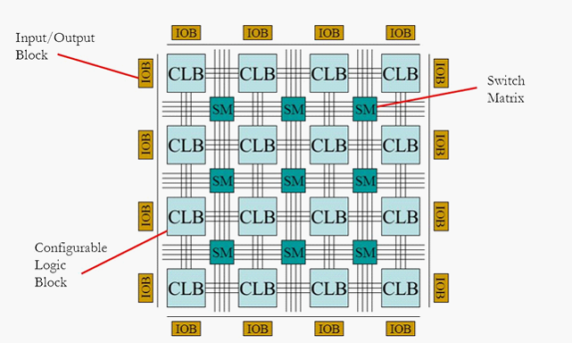
Logic Elements
The core of an FPGA is an array of configurable logic blocks that can be arranged in any manner desired.
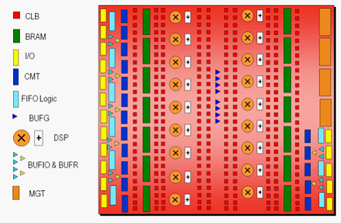
Configurable Logic Blocks (CLBs)
In modern Xilinx FPGAs (like Kintex-7 used in many SCI-Compiler boards), each CLB contains Slices with the following elements:
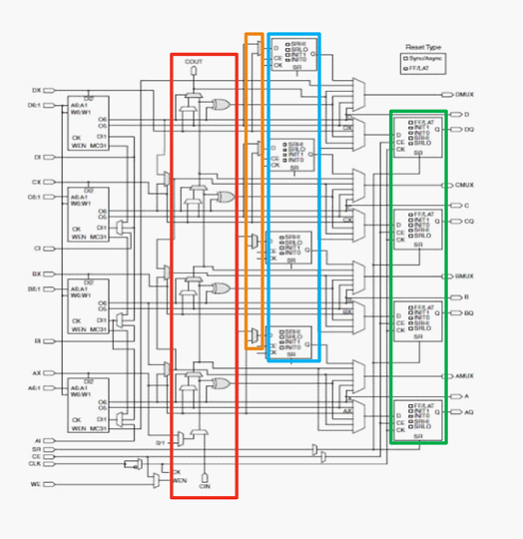
| Component | Quantity per Slice | Function |
|---|---|---|
| LUTs | 4 × 6-input | Implement any combinational logic function |
| Flip-Flops | 8 | Store data, implement sequential logic |
| Carry Chain | 1 | Accelerate arithmetic operations |
| Multiplexers | Several | Select between signals |
Look-Up Tables (LUTs)
LUTs are the fundamental building blocks for implementing logic. A 6-input LUT can implement any Boolean function of 6 variables by storing the truth table in memory:
6-Input LUT (64 entries):
Inputs: A, B, C, D, E, F (6 bits = 64 combinations)
Output: Programmable for each combination
Example: Implementing (A AND B) OR (C AND D)
Address [FEDCBA] | Output
------------------|--------
000000 | 0
000011 | 1 (A=1, B=1 → A AND B = 1)
001100 | 1 (C=1, D=1 → C AND D = 1)
... | ...
Why LUTs are powerful:
- Any 6-input function in one clock cycle
- Constant delay regardless of function complexity
- Can be combined for larger functions
Memory Resources
Block RAM (BRAM)
FPGAs contain dedicated memory blocks for efficient data storage:
| Feature | Typical Specification |
|---|---|
| Size per block | 18 Kb or 36 Kb |
| Configurations | Single-port, Dual-port, True dual-port |
| Width × Depth | Configurable (1×36K to 36×1K) |
| Access time | 1 clock cycle |
Common uses in SCI-Compiler:
- Waveform buffers (Oscilloscope, Digitizer)
- Histogram memory (Spectrum)
- FIFO buffers (List, Custom Packet)
- Coefficient tables (Filters)
Distributed RAM
LUTs can also be configured as small RAM blocks:
- 64 bits per LUT
- Very fast access
- Good for small lookup tables
Arithmetic Resources
DSP Blocks (DSP48E1)
Modern FPGAs include hardened DSP blocks optimized for signal processing:
DSP48E1 Block Diagram:
A[29:0] ──────►┌─────────┐
│ Pre- │
B[17:0] ──────►│ Adder │──►┌──────────┐
└─────────┘ │ │
│ Multiply │──►┌──────────┐
C[47:0] ─────────────────────►│ 25×18 │ │ ALU │──► P[47:0]
└──────────┘ │ Add/Sub │
│ Acc/Logic│
P (feedback) ──────────────────────────────►└──────────┘
| Operation | Performance |
|---|---|
| Multiply | 25 × 18 bit in 1 cycle |
| Multiply-Accumulate | (A × B) + C in 1 cycle |
| Maximum clock | 500+ MHz |
Used in SCI-Compiler for:
- Digital filters (Trapezoidal, CR-RC², Gaussian)
- FFT computations
- Baseline calculations
- Energy computations
Clock Resources
Clock Management
FPGAs include sophisticated clock resources:
| Resource | Function |
|---|---|
| Global Clock Buffers | Distribute clocks with minimal skew |
| PLLs/MMCMs | Generate clocks at different frequencies |
| Clock Regions | Partition clock domains |
Multiple Clock Domains
Real systems often use multiple clocks:
Example: DT5560 Clock Domains
CLK_SYS (100 MHz) ──► System logic, USB interface
CLK_ACQ (125 MHz) ──► ADC sampling, signal processing
CLK_DDR (200 MHz) ──► DDR memory interface
Clock domain crossing requires special care to avoid metastability. SCI-Compiler handles this automatically for you.
I/O Resources
High-Speed I/O
Modern FPGAs support various I/O standards:
| Standard | Speed | Application |
|---|---|---|
| LVDS | 1.25 Gbps | ADC interfaces |
| LVTTL/LVCMOS | 200 MHz | Digital I/O |
| GTX/GTH | 12.5 Gbps | High-speed serial (PCIe, SFP) |
| DDR3/DDR4 | 1600 MT/s | External memory |
SerDes Transceivers
High-speed serial transceivers enable:
- PCIe communication
- Ethernet interfaces
- Fiber optic links
- Multi-board synchronization
Hard IP Blocks
Modern FPGAs include hardened IP for common functions:
| Hard IP | Function |
|---|---|
| PCIe | PCI Express interface |
| Ethernet MAC | Network communication |
| Memory Controllers | DDR3/DDR4 interface |
| ARM Cores | Embedded processors (in SoC FPGAs) |
| XADC | Analog-to-digital conversion |
These hard blocks are more efficient than implementing the same function in programmable logic.
FPGA vs Other Technologies
FPGA vs CPU
| Aspect | FPGA | CPU |
|---|---|---|
| Execution | Parallel (all at once) | Sequential (instruction by instruction) |
| Latency | Nanoseconds (deterministic) | Microseconds to milliseconds |
| Throughput | Very high (custom datapath) | Limited by instruction rate |
| Power | Moderate | Higher for same throughput |
| Flexibility | Reconfigurable | Fixed architecture |
| Development | Longer, specialized | Faster, more familiar |
FPGA vs ASIC
| Aspect | FPGA | ASIC |
|---|---|---|
| Development cost | Low | Very high (mask costs) |
| Unit cost | Higher | Lower (at volume) |
| Time to market | Fast | Slow (months to years) |
| Reconfigurability | Yes | No |
| Performance | Good | Best |
| Power efficiency | Good | Best |
FPGAs are ideal when:
- Requirements may change
- Production volumes are low to medium
- Time to market is critical
- Real-time performance is needed
Classical FPGA Design Flow
Traditional FPGA development follows these stages:
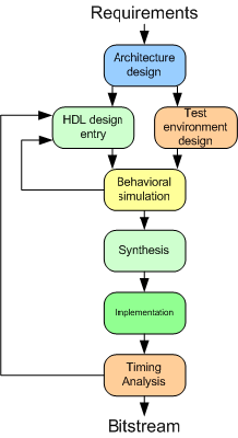
1. Architecture Design
- Analyze project requirements
- Decompose problem into functional blocks
- Define interfaces between blocks
- Functional simulation (if applicable)
Output: Architecture document describing the device structure
2. HDL Design Entry
The device is described in a Hardware Description Language (HDL):
| Language | Characteristics |
|---|---|
| VHDL | Strongly typed, verbose, common in Europe |
| Verilog | C-like syntax, common in USA/Asia |
| SystemVerilog | Extended Verilog with verification features |
Example VHDL code:
vhdl
-- Simple counter
process(clk, reset)
begin
if reset = '1' then
count <= (others => '0');
elsif rising_edge(clk) then
if enable = '1' then
count <= count + 1;
end if;
end if;
end process;
3. Simulation
Test the design before hardware:
- Write testbenches
- Apply stimulus
- Verify outputs match expected behavior
- Check timing relationships
4. Synthesis
Convert HDL to a netlist (digital circuit schematic):
- Map logic to LUTs and registers
- Optimize for area, speed, or power
- Report resource utilization
5. Implementation (Place & Route)
Map the netlist onto physical FPGA resources:
- Placement: Assign logic to specific CLBs
- Routing: Connect signals through interconnect
- Optimization: Meet timing constraints
6. Timing Analysis
Verify the design meets timing requirements:
- Setup time: Data arrives before clock
- Hold time: Data stable after clock
- Clock frequency: Design meets target speed
7. Bitstream Generation
Create the configuration file that programs the FPGA.
Why SCI-Compiler Simplifies This
The traditional FPGA design flow requires:
- Months to learn HDL
- Deep understanding of hardware concepts
- Experience with timing constraints
- Knowledge of FPGA architecture
SCI-Compiler eliminates these barriers:
| Traditional Flow | SCI-Compiler |
|---|---|
| Write HDL code | Draw block diagram |
| Design testbench | Use integrated simulator |
| Run synthesis | Automatic |
| Fix timing errors | Handled by certified IP |
| Write software driver | SciSDK generated automatically |
You focus on what you want to accomplish, not how to implement it at the hardware level.
Summary
FPGAs provide the perfect platform for real-time signal processing:
- Massive parallelism for high throughput
- Deterministic timing for precise measurements
- Reconfigurability for evolving requirements
- Custom datapaths for optimal efficiency
SCI-Compiler makes this powerful technology accessible to scientists and engineers without requiring FPGA expertise. You describe your algorithm graphically, and SCI-Compiler handles all the complexity of FPGA implementation.