Getting Started with FPGA Simulation
Step-by-step tutorial for FPGA simulation in SCI-Compiler. Learn to generate stimulus signals, configure registers, place probes, run simulation with Vivado, and analyze results with GTKWave. Verify your firmware design before hardware implementation to save time and identify issues early.
Introduction
Simulation is a critical step in FPGA development that allows you to verify the behavior of your design before implementing it on hardware. This can save significant time and resources by identifying and correcting issues early in the development process.
Why Simulate?
Benefits of simulation:
- Early bug detection - Find issues before hardware programming
- Algorithm verification - Confirm processing logic works correctly
- Timing analysis - Verify signal timing and synchronization
- Resource savings - Avoid repeated compilation cycles
- Complete visibility - Access all internal signals and nets
- Repeatability - Run the same test multiple times consistently
What You’ll Learn
- Understanding the FPGA simulation workflow
- Creating stimulus signals for ADC inputs
- Using the integrated signal generator
- Configuring registers for simulation
- Placing probes to monitor internal signals
- Running simulation with Vivado
- Viewing waveforms with GTKWave
- Analyzing analog and digital signals
- Debugging firmware designs
The Simulation Process
The FPGA simulation workflow consists of several key steps:
1. Design Creation
Create your digital design using SCI-Compiler’s graphical block diagram interface.
2. Testbench Creation
SCI-Compiler automatically generates the testbench code that:
- Provides stimulus to the design
- Configures registers
- Captures output signals
- Verifies expected results
3. Simulation Setup
Configure simulation parameters:
- Stimulus sources
- Register initial values
- Probe placements
- Simulation duration
4. Simulation Execution
The simulation tool (Vivado) executes the design and generates waveforms showing all signals over time.
5. Debugging
Examine waveforms to verify behavior. If results don’t match expectations, modify the design and repeat.
6. Iteration
The process may need to be repeated multiple times until the design behaves as expected.
SCI-Compiler Automation
SCI-Compiler manages all simulation steps automatically, leaving you only the task of:
- Generating stimulus signals
- Configuring initial register values
- Placing probes for signals of interest
- Debugging your algorithm
Important: Please read the Simulation Limitations topic to understand constraints and supported features.
Tutorial: Simulating a QDC Design
This tutorial uses the QDC (Charge-to-Digital Converter) example for DT1260. The same process applies to any custom project.
What this design includes:
- Leading edge trigger module
- Charge integrator (QDC)
- Configuration registers
- Oscilloscope endpoint
- Spectrum endpoint
Note: During simulation, Oscilloscope and Spectrum endpoints are automatically excluded. You can directly access all signals (waveforms and energy lists) produced by processing algorithms.
Step 1: Start from an Example Design
Create the Project
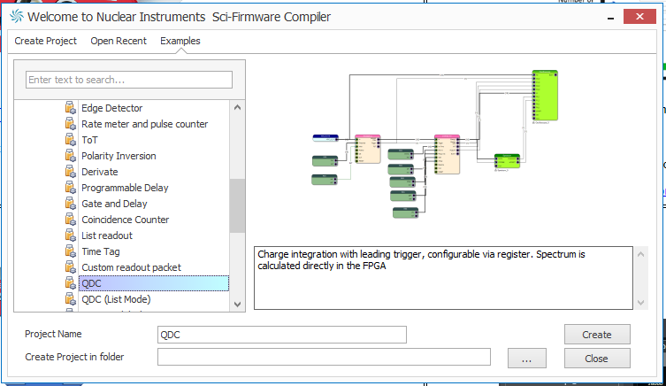
Figure 1: Opening the QDC example project
- Click File → New Project → From Example
- Navigate to the DT1260 folder
- Select QDC example
- Specify the project folder on your hard disk
- Click Create
Examine the Block Diagram
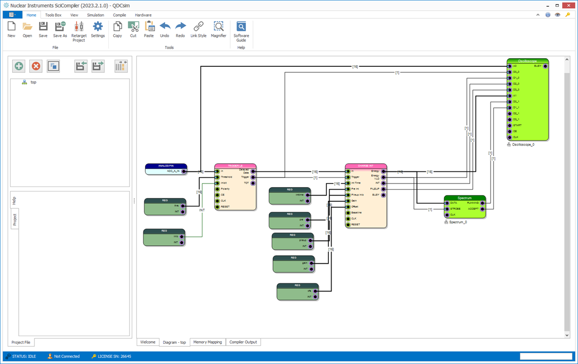
Figure 2: QDC firmware block diagram
The design contains:
- Board Analog Input (A0) - ADC channel input
- Leading Edge Trigger - Detects signal threshold crossing
- Charge Integrator (QDC) - Measures pulse energy
- Configuration Registers - Threshold, gate width, etc.
- Oscilloscope - Waveform capture (excluded in simulation)
- Spectrum - Energy histogram (excluded in simulation)
Step 2: Generate Stimulus
Stimulus signals are fake input signals that replace real ADC analog signals during simulation. They simulate the operational conditions of your detector or signal source.
What is Stimulus?
The stimulus represents your detector signal used as input for simulation:
- Can be loaded from a CSV file (one value per row)
- Can be generated using SCI-Compiler’s integrated signal generator
For this example, we’ll use the integrated signal generator.
Add Stimulus to Analog Input
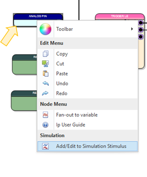
Figure 3: Adding simulation stimulus
- Right-click on the Analog Pin box (A0)
- Select Add/Edit Simulation Stimulus
Configure Signal Generator
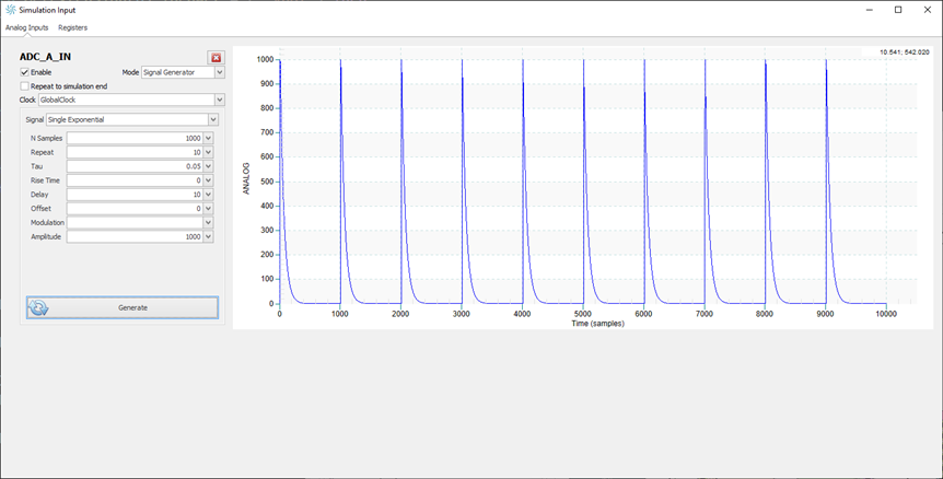
Figure 4: Signal generator configuration
- Set Mode to Signal Generator
- Set Signal to Single Exponential (typical scintillator pulse)
- Configure parameters:
- Amplitude - Peak signal value
- Rise Time - Signal rise time constant
- Decay Time - Signal decay time constant (e.g., 1 µs for NaI)
- Baseline - DC offset
- Noise - Add random noise
- Number of Pulses - How many pulses to generate
- Pulse Interval - Time between pulses
- Click Generate
The tool generates a waveform preview and creates the stimulus file.
Alternative: Load from File
To use a custom CSV file:
- Set Mode to From File
- Browse to your CSV file
- CSV format: one ADC value per line (decimal or hex)
0 10 50 200 500 ...
Step 3: Set the Registers
Registers contain configuration for processing algorithms. All registers must be initialized before simulation runs.
Why Configure Registers?
During simulation, you can:
- Initialize all registers to default values
- Change register values at specific times
- Test different parameter configurations
- Verify register-based control logic
Write Register Script
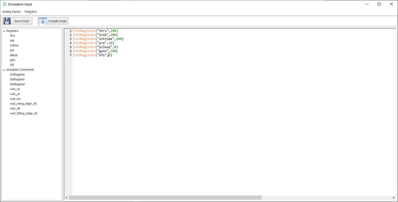
Figure 5: Register initialization script
- Click the Registers tab in simulation settings
- Write initialization script using available commands:
Available commands:
InitRegister <name> <value>- Initialize a registerSetRegister <name> <value>- Change register value during simulationwait_us <microseconds>- Wait for specified timewait_ns <nanoseconds>- Wait for specified timewait_clk <cycles>- Wait for clock cycles
Example Script
InitRegister threshold 100
InitRegister gate_width 500
InitRegister pretrigger 50
InitRegister polarity 1
wait_us 10
SetRegister threshold 150
wait_us 20
SetRegister threshold 200
Left panel shows:
- List of available registers in your design
- Valid command syntax
- Current register values
Step 4: Place Probes
Probes are labeled observation points that make internal signals easily accessible in waveform viewers.
Why Use Probes?
- Simulation produces output files containing all internal nets
- Without probes, finding specific signals is difficult
- Probes give clear labels to important signals
- Probes bring signals to the top level of the design hierarchy
- Makes debugging much faster and easier
Add Probe Blocks
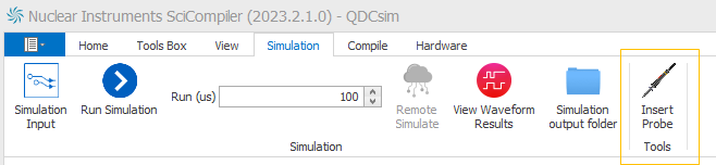
Figure 6: Adding probe from Simulation Toolbox
- Open Simulation Toolbox menu
- Click Probe tool
- Place probe block on the diagram
- Connect to the signal you want to monitor
Configure Probe Properties
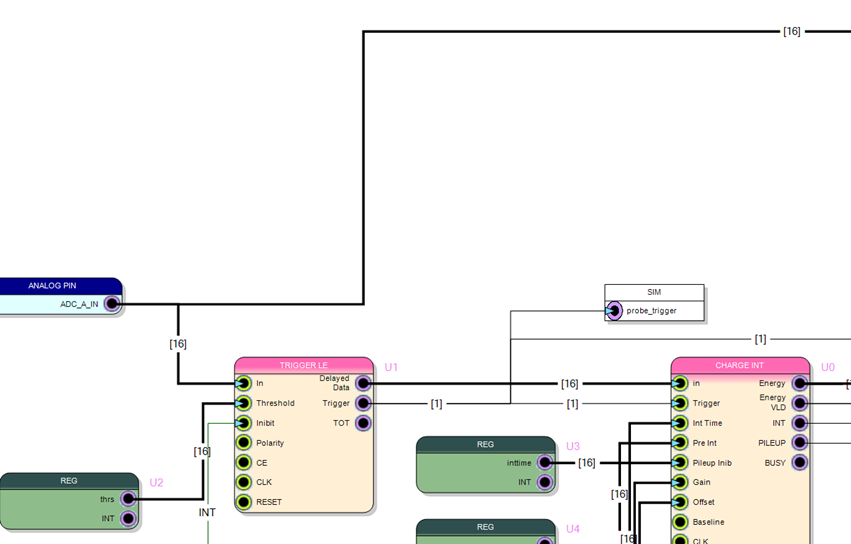
Figure 7: Configuring probe name
- Double-click the probe block
- Set Probe Name (e.g., “trigger”, “energy”, “valid”)
- Click OK
Example Probe Placements
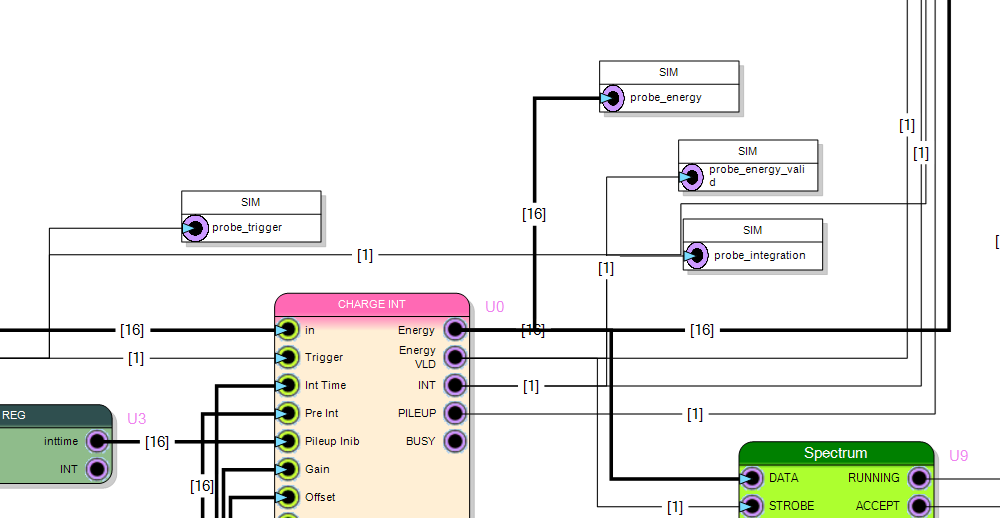
Figure 8: Multiple probes placed on the design
For the QDC example, place probes on:
- A0 - Analog input stimulus
- trigger - Trigger output from threshold detector
- integration - Integration gate signal
- energy - Energy value output from QDC
- energy_valid - Energy data valid flag
Tip: Use descriptive names that clearly indicate the signal’s function.
Step 5: Run Simulation
Prerequisites
Required software:
- Xilinx Vivado must be installed on your local machine
- SCI-Compiler automatically detects Vivado installation
- Simulation uses Vivado’s xsim simulator
Start Simulation
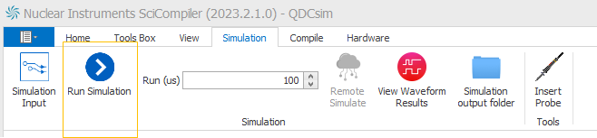
Figure 9: Starting the simulation
- Click Run Simulation button in the Home toolbar
- SCI-Compiler generates:
- VHDL testbench code
- Stimulus files
- TCL scripts for Vivado
- Vivado is launched automatically
- Compilation and simulation begin
Monitor Progress
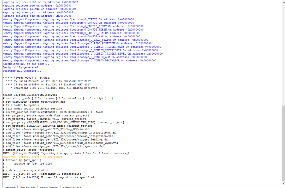
Figure 10: Simulation progress log
The Simulation Output tab shows:
- VHDL compilation messages
- Testbench generation status
- Simulation execution progress
- Any warnings or errors
- Completion status
Typical simulation time: 1-5 minutes depending on:
- Design complexity
- Simulation duration
- Computer performance
Step 6: View Waveform Results
Launch GTKWave
SCI-Compiler uses GTKWave, an open-source waveform viewer, to display simulation results. GTKWave is automatically installed with SCI-Compiler.
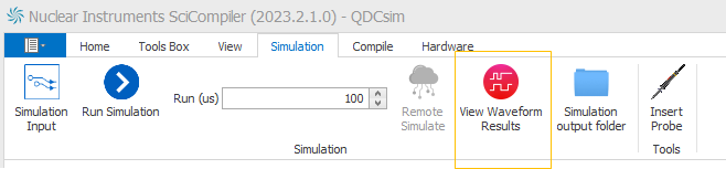
Figure 11: Opening waveform viewer
- Click View Waveform Results button
- GTKWave launches automatically
- Simulation waveform file (.vcd or .ghw) is loaded
Select Signals to Display
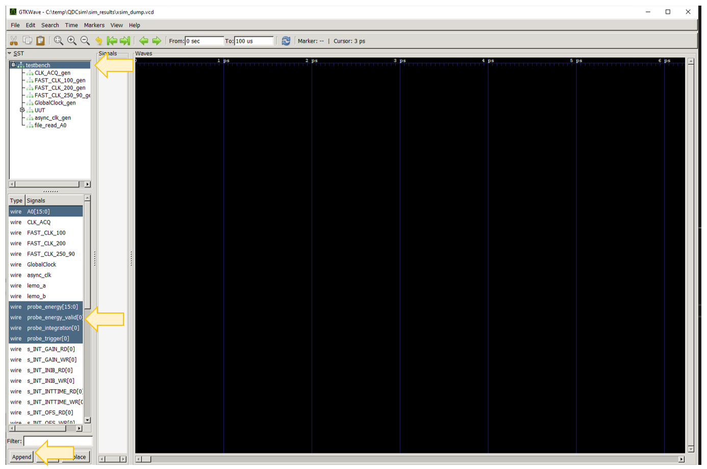
Figure 12: Selecting signals in GTKWave
GTKWave interface:
- SST (Signal Search Tree) - Left panel showing design hierarchy
- Signals - Middle panel listing available signals
- Waveform display - Right panel showing signal traces
To add signals:
- Click on testbench in the SST column
- Locate your probe signals in the middle panel
- Select signals you want to view
- Click Append button (or drag to waveform area)
Zoom to View Full Simulation
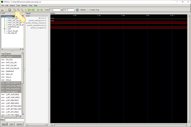
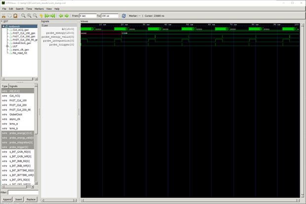
Figure 13: Zoom controls and full waveform
Use the Zoom Fit button (or press Ctrl+Alt+F) to see the entire simulation time range.
Other zoom controls:
- Zoom In - Magnify time axis
- Zoom Out - Show more time
- Zoom to Selection - Focus on highlighted region
- Mouse wheel - Zoom in/out at cursor
Step 7: Format Digital Signals
By default, multi-bit signals display in hexadecimal. You can change the format to decimal, binary, or other representations.
Change to Decimal Format
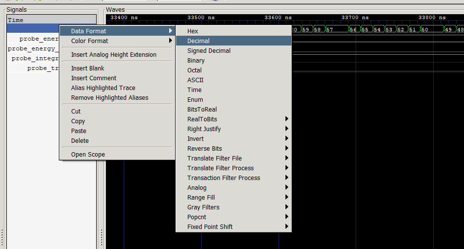
Figure 14: Changing signal format to decimal
- Right-click on the signal trace (e.g., A0)
- Select Data Format → Decimal
- Signal values now display as decimal numbers
Available formats:
- Hex - Hexadecimal (default)
- Decimal - Signed decimal
- Unsigned Decimal - Unsigned decimal
- Binary - Binary bits
- Octal - Octal representation
- ASCII - Character encoding
Step 8: View Analog Plot
For analog signals like ADC inputs, you can display them as continuous waveforms rather than digital traces.
Increase Signal Height
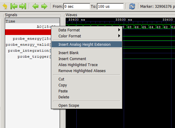
Figure 15: Increasing analog signal display height
- Right-click on the signal trace (e.g., A0)
- Select Insert Analog Height Extension
- Repeat 5-6 times to create sufficient vertical space
Enable Analog Display Mode
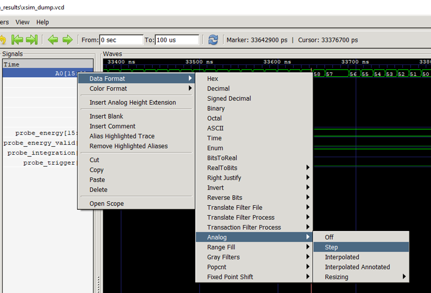
Figure 16: Selecting analog step format
- Right-click on the signal trace
- Navigate to Data Format → Analog → Step
- The signal now displays as an analog waveform
Analog display modes:
- Step - Step interpolation (recommended for sampled signals)
- Interpolated - Linear interpolation between samples
- Real - For floating-point values
Result: Analog Waveform
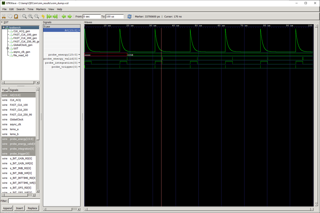
Figure 17: Final analog waveform display
You can now see:
- A0 analog input - Exponential pulse shape
- Trigger output - Goes high when threshold exceeded
- Integration gate - Active during charge integration
- Energy value - Final integrated charge
- Energy valid - Indicates new energy value available
Analyze Signal Relationships
Using GTKWave cursors:
- Primary cursor (orange) - Click on waveform
- Secondary cursor (green) - Middle-click on waveform
- Time measurement - Shown between cursors
Verify:
- Trigger latency after threshold crossing
- Integration gate width matches register setting
- Energy value correlates with pulse amplitude
- Timing relationships between signals
Advanced Simulation Techniques
Custom Stimulus Files
Create realistic detector signals:
python
# Python script to generate complex stimulus
import numpy as np
# Parameters
sample_rate = 125e6 # 125 MHz
pulse_rate = 10e3 # 10 kHz pulses
amplitude = 2000
decay = 1e-6 # 1 µs decay
# Generate pulse train
time = np.arange(0, 1e-3, 1/sample_rate)
signal = np.zeros_like(time)
for t_pulse in np.arange(0, 1e-3, 1/pulse_rate):
idx = int(t_pulse * sample_rate)
pulse = amplitude * np.exp(-(time[idx:] - t_pulse) / decay)
signal[idx:] += pulse[:len(signal)-idx]
# Add noise
signal += np.random.normal(0, 10, len(signal))
# Save as CSV
np.savetxt('stimulus.csv', signal.astype(int), fmt='%d')
Dynamic Register Changes
Test parameter sweeps during simulation:
InitRegister threshold 50
wait_us 100
SetRegister threshold 100
wait_us 100
SetRegister threshold 150
wait_us 100
SetRegister threshold 200
wait_us 100
Multiple Input Channels
For multi-channel designs:
- Add stimulus to each analog input
- Use different signal patterns per channel
- Place probes on each channel’s outputs
- Verify channel independence and crosstalk
Probe Arrays
Monitor bus signals efficiently:
- Place probe on multi-bit signal
- GTKWave shows entire bus
- Expand bus to view individual bits
- Use appropriate data format (hex/decimal/binary)
Saving GTKWave Sessions
Save your signal selection and formatting:
- Configure signals, zoom, cursors
- File → Write Save File (.gtkw)
- Next time: File → Read Save File
- All settings restored automatically
Simulation Limitations
Excluded Components
Some SCI-Compiler blocks cannot be simulated:
- Oscilloscope endpoints (use probes instead)
- Spectrum endpoints (use probes on energy values)
- List endpoints (use probes on event data)
- USB/Network communication (testbench replaces)
- Board-specific peripherals (I2C, SPI controllers)
Simplified Models
Some blocks use simplified behavior models:
- ADC inputs use stimulus files
- Clock sources are idealized
- External triggers simulated as internal signals
- Memory endpoints may have limited depth
Timing Accuracy
Simulation uses:
- Functional timing (default) - Faster, no gate delays
- Post-synthesis timing - Optional, includes routing delays
For most algorithm debugging, functional timing is sufficient.
Simulation Duration
Longer simulations require:
- More disk space for waveform files
- More time to run
- More time to load in GTKWave
Recommended: Start with short simulations (10-100 µs) and increase as needed.
Troubleshooting
Simulation Fails to Start
Problem: Vivado not found or simulation errors
Solutions:
- Verify Vivado is installed and in PATH
- Check SCI-Compiler → Settings → Simulation paths
- Ensure Vivado license is valid
- Review error messages in Simulation Output
No Stimulus Visible
Problem: Analog input shows all zeros
Solutions:
- Verify stimulus file was generated
- Check stimulus amplitude (not too small)
- Ensure stimulus file path is correct
- Try regenerating stimulus with signal generator
Probes Not Appearing
Problem: Cannot find probe signals in GTKWave
Solutions:
- Verify probes were added to block diagram
- Check probe names are valid (no spaces/special chars)
- Look in testbench hierarchy in GTKWave
- Ensure simulation completed successfully
Waveform File Too Large
Problem: GTKWave slow or crashes loading waveform
Solutions:
- Reduce simulation duration
- Use fewer probes (only essential signals)
- Enable waveform compression in Vivado
- Increase system RAM
- Use VCD instead of FST format (smaller)
Wrong Register Values
Problem: Algorithm behaves incorrectly
Solutions:
- Verify InitRegister values are correct
- Check register addresses match your design
- Ensure all required registers are initialized
- Add probe on register outputs to verify
Timing Issues
Problem: Signals not synchronized correctly
Solutions:
- Check clock domain crossings
- Verify delay/pipeline stages
- Use cursors to measure actual timing
- Compare to expected timing calculations
- Enable post-synthesis timing simulation
Best Practices
Start Simple
- Begin with basic stimulus (single pulse)
- Verify basic functionality
- Add complexity gradually (multiple pulses, noise)
- Test edge cases
Use Descriptive Probe Names
Good probe names:
adc_inputtrigger_outenergy_valueevent_valid
Avoid:
probe1,probe2signal,out- Single letters
Document Expected Behavior
Before simulation:
- Calculate expected results manually
- Estimate timing (latency, gate widths)
- Write down expected signal patterns
- Compare simulation results to expectations
Verify Critical Paths
Always probe:
- Trigger signals - Verify threshold detection
- Data valid flags - Confirm processing completion
- Output values - Check calculation accuracy
- State machines - Verify state transitions
- Error conditions - Test fault handling
Automate Verification
For complex designs:
- Use scripted stimulus generation
- Create reference calculations in Python/Matlab
- Export waveform data from GTKWave
- Compare against reference
- Automate pass/fail checking
Summary
This tutorial covered the complete FPGA simulation workflow in SCI-Compiler:
| Step | Action | Tool |
|---|---|---|
| 1 | Open example or create design | SCI-Compiler |
| 2 | Generate stimulus signals | Signal Generator |
| 3 | Initialize registers | Register Script |
| 4 | Place probes on signals | Probe Tool |
| 5 | Run simulation | Vivado xsim |
| 6 | View waveforms | GTKWave |
| 7 | Format signals | GTKWave |
| 8 | Display analog plots | GTKWave |
| 9 | Analyze and debug | Manual verification |
Key Takeaways:
- Simulation verifies firmware before hardware implementation
- SCI-Compiler automates testbench generation
- Stimulus files replace real ADC inputs
- Probes make internal signals easily accessible
- GTKWave provides powerful waveform analysis
- Iterative debugging improves design quality
Next Steps:
- Simulate your own custom designs
- Create realistic stimulus files for your detectors
- Experiment with parameter sweeps
- Verify timing relationships
- Test edge cases and error conditions
- Build automated verification scripts
- Use simulation to optimize algorithms
- Debug complex multi-channel designs
Simulation is essential for professional FPGA development. Master it to create reliable, high-quality firmware designs!