
Fixed Delay
Synchronous fixed delay line that delays the input signal by a user-configured number of clock cycles. Uses FPGA registers for storage and provides deterministic, fixed-latency delay. Suitable for clock-cycle-precise timing adjustments in digital signal processing pipelines.
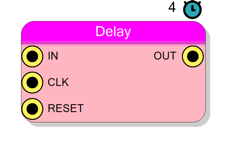
Introduction
This block implements a digital fixed delay line using FPGA registers to delay an input signal by a predetermined number of clock cycles. The delay value is set at design time and cannot be changed during runtime.
The delay is synchronous and clocked:
$$ \mathrm{OUT}(n) = \mathrm{IN}(n - D), $$
where $D$ is the Delay Value property (in clock cycles). The block provides deterministic latency equal to $D$ clock cycles.
Pin Description
Bit Width bits (1-1024)
The input is sampled on every rising edge of CLK.
Delayed output data signal.
Width: Bit Width bits (same as IN)
OUT(n) = IN(n - Delay Value)
Output is registered and valid on the rising edge of CLK.
Properties
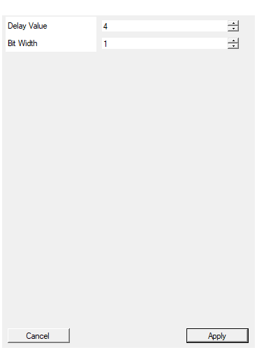
Set the delay in clock cycles introduced by the delay line
Number of clock cycles to delay the input signal. Range: 1 – 1024 clock cycles.
This value is fixed at compile time and determines the component’s latency.
The delay line requires DelayValue × BusWidth FPGA flip-flops.
For delays > 16 cycles, consider using the Variable Delay block which uses block RAM instead of registers.
Default: 4
Range: 1 – 1024
Set the size in bits of the signal to be delayed
Bit width of the input/output signals. Range: 1 – 1024 bits.
Total flip-flop usage = BusWidth × DelayValue.
Default: 1
Range: 1 – 1024
Functional description
The component uses a shift register implementation built from FPGA flip-flops (registers). On each rising edge of CLK, the input value is shifted into the delay line, and the value that was stored $D$ clock cycles ago emerges at the output.
Implementation details
- Storage: Uses FPGA registers (flip-flops), not block RAM
- Latency: Exactly $D$ clock cycles
- Reset behavior: When RESET=‘1’, the delay line is cleared
- Resource usage: Consumes
Bit Width × Delay Valueflip-flops
When to use Fixed Delay vs Variable Delay
Use Fixed Delay when:
- Delay value is known at compile time and never changes
- Delay is relatively small (< 16 clock cycles typically)
- You need the most efficient hardware implementation
Use Variable Delay (programmable) when:
- Delay needs to change at runtime
- Delay is larger (> 16 clock cycles)
- You can afford the extra 1-cycle latency overhead
Timing
The component has fixed latency equal to the Delay Value property:
| Property | Latency (clock cycles) |
|---|---|
| Fixed Delay | D |
where $D$ is the configured delay value (1-1024 clock cycles).
Typical use cases
- Clock-domain crossing alignment: Matching propagation delays across parallel paths
- Pipeline stage balancing: Equalizing latencies in multi-path architectures
- Timing compensation: Compensating for combinational logic delays
- Synchronization: Aligning data streams for coincidence detection
Design considerations
Resource usage
For large delays or wide data paths, consider using the Variable Delay block instead, which uses block RAM and is more resource-efficient for delays > 16 cycles.
Example resource usage:
- 8-bit delay of 4 cycles: 32 flip-flops
- 16-bit delay of 10 cycles: 160 flip-flops
- 32-bit delay of 100 cycles: 3200 flip-flops (use Variable Delay instead!)
Waveform example
Example with Delay Value = 4, Bit Width = 1.
Note: OUT follows IN with exactly 4 clock cycle delay.